
1. Introduction
This manual provides essential information for the proper use and handling of your GENNEL 50x70mm Copper Strip PCB Boards. These universal stripboards are designed for prototyping, testing, and building electronic circuits. Please read these instructions carefully to ensure optimal performance and longevity of your projects.
2. Product Features
- Material: The base material is fiberglass, providing enhanced strength and durability.
- Dimensions: Each board measures 50mm x 70mm x 1.0mm (approximately 1.96" x 2.75" x 0.04").
- Configuration: Single-sided stripboard design.
- Hole Specifications: Features 23 copper tracks, each with 16 holes, totaling 368 holes. Hole pitch is 2.54mm (0.1 inch), and hole diameter is 1.0mm.
- Solder Mask: The surface between holes and strips is covered with a green coating for solder mask, preventing solder bridging and simplifying operations.
- Versatility: Suitable for soldering various electronic components such as connectors, LEDs, sensors, and resistors.

Image 2.1: A stack of GENNEL 50x70mm Copper Strip PCB Boards, illustrating the quantity and standard appearance.
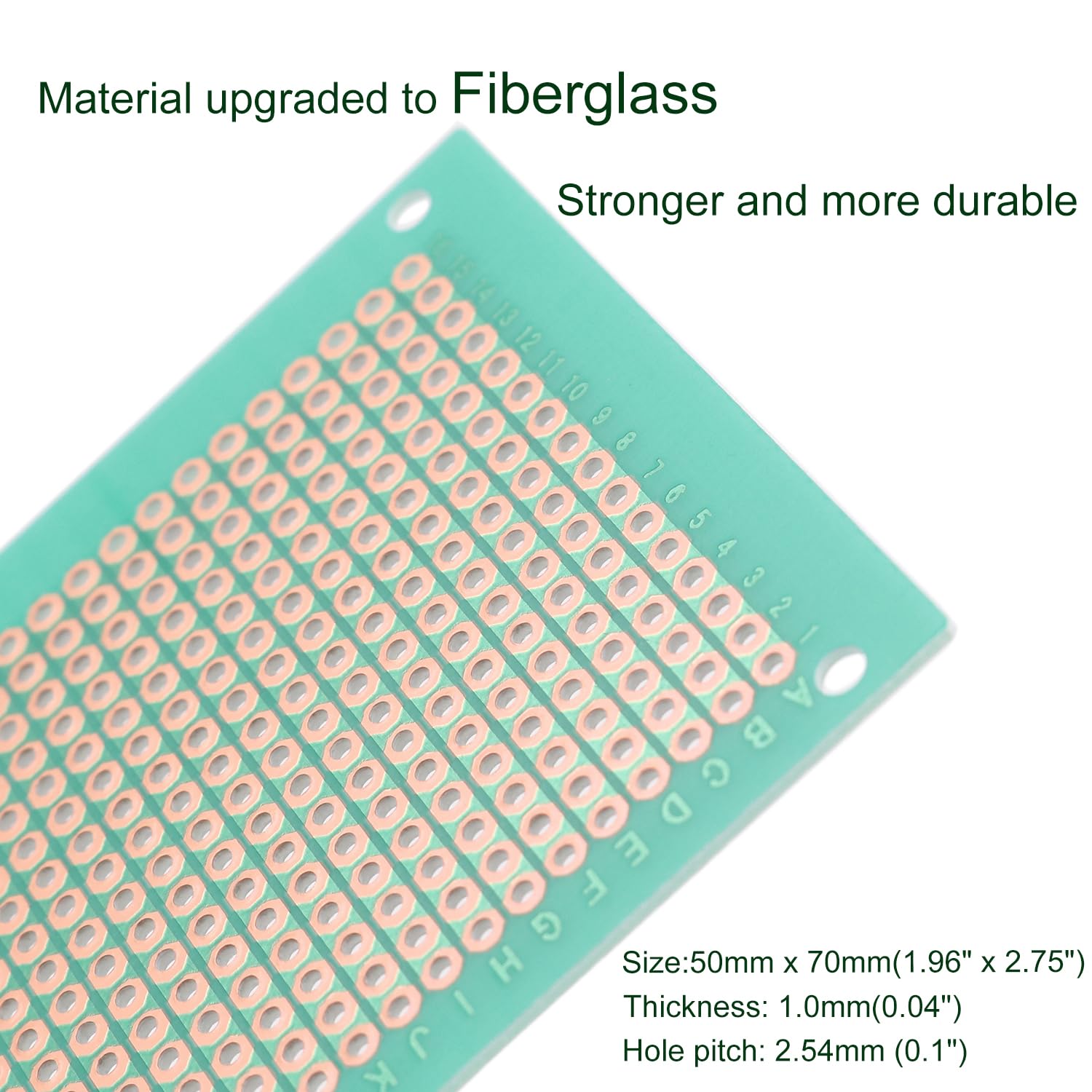
Image 2.2: Close-up view of a GENNEL PCB board, emphasizing the fiberglass material and precise dimensions (50mm x 70mm, 1.0mm thickness, 2.54mm hole pitch).
3. Setup and Preparation
Before beginning your project, ensure you have all necessary tools, including a soldering iron, solder, flux, wire cutters, and safety glasses.
3.1. Board Handling
- Handle boards by the edges to avoid transferring oils or dirt to the copper traces.
- Store boards in a dry, clean environment to prevent oxidation.
3.2. Cutting the Board (Optional)
If your project requires a smaller board size, the stripboard can be cut. To do this:
- Mark the desired cut line clearly on the board.
- Using a sharp utility knife and a ruler, score the board along the marked line multiple times until a deep groove is formed.
- Carefully snap the board along the scored line. For best results, place the scored line over the edge of a table and apply even pressure.
3.3. Preparing for Soldering
While the boards feature a solder mask, applying a small amount of flux to the pads before soldering can improve solder flow and joint quality, especially for components with larger leads or if you are new to soldering.

Image 3.1: A detailed view of the stripboard surface, highlighting the green solder mask that covers the areas between holes and strips, designed to prevent solder bridges.
4. Operating Instructions (Soldering)
These stripboards are ideal for point-to-point wiring of electronic components. Each row of holes is connected by a copper strip on one side, allowing for easy component placement and connection.
4.1. Component Placement
- Insert component leads into the desired holes. Ensure components are placed according to your circuit diagram.
- Bend the leads slightly on the copper side to hold the component in place before soldering.
4.2. Soldering Technique
- Heat the component lead and the copper pad simultaneously with the tip of your soldering iron.
- Apply a small amount of solder to the heated joint. The solder should flow smoothly around the lead and pad, forming a shiny, cone-shaped joint.
- Remove the solder, then remove the soldering iron. Allow the joint to cool naturally.
- Trim excess component leads with wire cutters.
4.3. Breaking Copper Tracks (Optional)
To create breaks in the copper strips for component isolation or circuit routing, you can use a small drill bit (e.g., 3mm) or a specialized track cutter. Gently twist the drill bit over the desired copper track to remove a small section of copper, effectively breaking the electrical connection.

Image 4.1: The underside of the PCB board, clearly showing the continuous copper traces that connect holes in each row, facilitating circuit construction.
5. Maintenance
These PCB boards require minimal maintenance. Keep them clean and dry. If any residue accumulates from soldering, it can be carefully removed with isopropyl alcohol and a soft brush or cloth.
6. Troubleshooting
6.1. Solder Not Sticking / Cold Joints
- Ensure your soldering iron tip is clean and properly tinned.
- Verify the soldering iron temperature is appropriate for your solder type.
- Apply a small amount of flux to the pad and component lead before applying solder.
- Ensure both the lead and pad are heated simultaneously before introducing solder.
6.2. Pads Lifting
- Avoid excessive heat or prolonged contact with the soldering iron. Apply heat only long enough for the solder to flow.
- Do not apply mechanical stress to components while the solder is still molten.
6.3. Solder Bridges
- The green solder mask helps prevent solder bridges. If one occurs, use solder wick or a desoldering pump to remove excess solder.
- Use less solder for each joint.
7. Specifications
| Feature | Specification |
|---|---|
| Model Number | GNCA57 |
| Dimensions (L x W x T) | 50mm x 70mm x 1.0mm (1.96" x 2.75" x 0.04") |
| Base Material | Fiberglass |
| Copper Tracks | 23 |
| Holes per Track | 16 |
| Total Holes | 368 |
| Hole Pitch | 2.54mm (0.1 inch) |
| Hole Diameter | 1.0mm |
| Surface Coating | Green Solder Mask |

Image 7.1: A side profile view of the PCB board, illustrating its thin and compact design.
8. Warranty and Support
For any questions, technical assistance, or support regarding your GENNEL Copper Strip PCB Boards, please contact GENNEL customer service through the retailer where the product was purchased. Please refer to your purchase documentation for specific warranty details, if applicable.