ANALOG DEVICES EVAL-LTM4683-A1Z Evaluation Board

Product Specifications
- Product Name: EVAL-LTM4683-A1Z
- Input Voltage Range: 4.5V to 14V
- Output Current: 31.25A per channel
- Switching Frequency: 350kHz
- Efficiency: Up to 86.4%
Product Usage Instructions
Quick Start
Required Equipment
- Input power supply
- Measurement equipment
Procedure
- Connect input power supply between VIN and GND, set voltage to 0V.
- Connect loads to VOUT0 to VOUT3, preset loads to 0A.
- Check jumpers and switches positions as per manual.
- Adjust input voltage between 6V to 14V and load current up to 31.25A per channel.
Measurement Techniques
To measure voltage ripples properly:
- Avoid using long ground leads on oscilloscope probes.
- Solder short, stiff leads to capacitor terminals for probe connections.
Frequently Asked Questions (FAQ):
- Q: What is the default input voltage range for EVAL-LTM4683-A1Z?
A: The default input voltage range is 4.5V to 14V. - Q: How can I monitor real-time performance?
A: Use LTpowerPlay software and the I2C/PMBus/SMBus dongle DC1613A for real-time monitoring.
Evaluation Board User Guide
EVAL-LTM4683-A1Z
LTM4683
Low VOUT Quad 31.25A (EVAL-LTM4683-A1Z) or Single 125A (EVAL-LTM4683-A2Z) µModule Regulator with Digital Power System Management
General Description
The EVAL-LTM4683-A1Z evaluation board features the LTM4683: the wide input and output voltage range, high efficiency and power density, quad output PolyPhase® DC-to-DC step-down µModule® (micromodule) regulator with digital power system management (PSM). The EVAL-LTM4683-A1Z evaluation board is configured as a 4-phase four outputs. A similar evaluation board with a 4-phase single output is also available (EVAL-LTM4683-A2Z).
The EVAL-LTM4683-A1Z evaluation board’s default input voltage range is 4.5V to 14V. However, if VIN is lower than 6V and within 4.5V ≤ VIN ≤ 5.75V, a minor modification to certain existing on-board components is required. See step 0 (Operation at Low VIN: 4.5V ≤ VIN ≤ 5.75V) in the Procedure section.
The factory default output voltage VOUT [0:3] is 0.4V at 31.25A maximum load current per channel. Each channel can deliver up to 31.25A maximum load current but forced airflow and heatsink might also be used to further optimize the output power when all output rails are on and fully loaded. The evaluation board output voltages can be adjusted from 0.3V up to 0.7V. Refer to the LTM4683 data sheet for thermal derating curves and recommended switching frequency when adjusting the output voltage. The factory default switching frequency is preset at 350kHz (typical). The EVAL-LTM4683-A1Z evaluation board comes with a PMBus interface and digital PSM functions. An on-board 12-pin connector is available for the users to connect the dongle DC1613A to the evaluation board, which provides an easy way to communicate and program the part using the LTpowerPlay® software development tool.
The LTpowerPlay software and the I2C/PMBus/SMBus dongle DC1613A allow the users to monitor real-time telemetry of input and output voltages, input, and output current, switching frequency, internal IC die temperatures, external power component temperatures, and fault logs. Programmable parameters include device address, output voltages, control loop compensation, switching frequency, phase interleaving, discontinuous-conduction mode (DCM) or continuous-conduction mode (CCM) of operation, digital soft start, sequencing, and time-based shutdown, fault responses to input and output overvoltage, output overcurrent, IC die and power component over temperatures.
The LTM4683 is available in a thermally enhanced, low-profile 330-pin, (15mm × 22mm × 5.71mm) BGA package. It is recommended to read the LTM4683 data sheet and this user guide prior to using or making any hardware changes to the EVAL-LTM4683-A1Z evaluation board.
Features and Benefits
- Quad digitally adjustable analog loops with digital interface for control and monitoring.
- Optimized for low output voltage ranges.
- 15mm × 22mm × 5.71mm BGA package.
EVAL-LTM4683-A1Z Evaluation Board
| FILE | DESCRIPTION |
| Design files. | |
| Easy-to-use Windows® based graphical user interface (GUI) development tool. | |
| DC1613A | The USB to PMBus controller dongle. |
Ordering Information appears at end of this user guide.
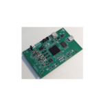
Evaluation Board Photo

Performance Summary
Specifications are at TA = 25°C
| PARAMETER | CONDITIONS | MIN | TYP | MAX | UNIT |
| Input Voltage VIN Range | 4.5 | 12 | 14 | V | |
| Evaluation board default output voltage, VOUT0–OUT3 | fSW = 350kHz, VIN = 4.5V to 14V,
IOUT = 0A to 31.25A per channel. |
0.4 |
V |
||
| Switching frequency, fSW | Factory default switching frequency. | 350 | kHz | ||
| Maximum continuous output current per channel, IOUT0–OUT3 |
30 |
31.25 |
A |
||
|
Efficiency |
fSW = 350kHz, VIN =12V, VOUT0 = 0.4V
IOUT0 = 0A to 31.25A, VBIAS = 5.5V (RUNP: ON), only one channel is on at a time, no forced airflow, no heatsink. |
79.1 |
% |
||
|
Thermal performance |
fSW = 350kHz, VIN =12V,
VOUT0–OUT3 = 0.4V, IOUT0–OUT3 = 31.25A per channel, VBIAS = 5.5V (RUNP: ON), no forced airflow, no heatsink. |
86.4 |
°C |
||
Quick Start Required Equipment
- One power supply that can deliver 20V at 20A.
- Four electronic loads that can deliver 35A at 0.3V each load.
- Five digital multimeters (DMMs).
Procedure
The EVAL-LTM4683-A1Z evaluation board is easy to set up to evaluate the performance of the LTM4683. See Figure 2 for proper measurement equipment setup and use the following test procedures.

- With power off, connect the input power supply between VIN (TP9) and GND (TP10). Set the input voltage supply to 0V.
- Connect the first load between VOUT0 (TP23) and GND (TP24), connect the second load between VOUT1 (TP20) and GND (TP21), connect the third load between VOUT2 (TP7) and GND (TP8), connect the fourth load between VOUT3 (TP5) and GND (TP6). Preset all the loads to 0A.
- Connect the DMM between the input test points: VIN (TP1) and GND (TP11) to monitor the input voltage. Connect DMMs between VOUT0+ (TP16) and VOUT0− (TP17), VOUT1+ (TP18) and VOUT1− (TP19), VOUT2+ (TP12) and VOUT2− (TP14), VOUT3+ (TP13) and VOUT3− (TP15) to monitor the corresponding dc output voltages of Channel 0, Channel 1, Channel 2, and Channel 3. These output voltage test points are Kelvin sensed directly across COUT2 (Channel 0), COUT10 (Channel 1), COUT20 (Channel 2), and COUT29 (Channel 3) to provide an accurate measurement of output voltages. Do not apply load current to any of the above test points to avoid damage to the regulator. Do not connect the scope probe ground leads to VOUT0−, VOUT1−, VOUT2−, and VOUT3−.
- Prior to powering up the EVAL-LTM4683-A1Z, check the default position of the jumpers and switches in the following positions.
SWITCH/JUMPER
SWR0, SWR1 SWR2, SWR3 P1
P2 P17 DESCRIPTION
RUN0, RUN1 RUN2, RUN3 RUNP
WP_01 WP_23 POSITION OFF ON OFF - Turn on the power supply at the input. Slowly increasing the input voltage from 0V to 12V (typical). Measure and make sure the input supply voltage is 12V and flip SWR0 (RUN0) and SWR1 (RUN1), SWR2 (RUN2), and SWR3 (RUN3) to the ON position. The output voltages should be 0.4V ±0.5% (typical) for VOUT0, VOUT1, VOUT2, and VOUT3.
- Once the input and output voltages are properly established, adjust the input voltage between 6V to 14V max and the load current within the operating range of 0A to 31.25A max per channel. Observe the output voltage regulation, output voltage ripples, switching node waveform, load transient response, and other parameters. See Figure 3 for proper output voltage ripples measurement.
To measure the input/output voltage ripples properly, do not use the long ground lead on the oscilloscope probe. See Figure 3 for the proper scope probe technique. Short, stiff leads need to be soldered to the (+) and (−) terminals of an input or output capacitor. The probe’s ground ring needs to touch the (−) lead, and the probe tip needs to touch the (+) lead.
The output voltage ripples of Channel 0, Channel 1, Channel 2, and Channel 3 can also be monitored using on-board BNC terminals. Connect short BNC cables from VOUT0 (J3), VOUT1 (J4), VOUT2 (J5), and VOUT3 (J6) to the inputs of a 4-channel oscilloscope (scope probe ratio 1:1, AC-coupling) to observe output voltage ripples. (Option) Operation with VBIAS
 - The VBIAS pin is the 5.5V output of an internal buck regulator that can be enabled or disabled with RUNP. The VBIAS regulator input is the VIN_VBIAS pin and is powered from VIN. The advantage of using VBIAS is bypassing the internal INTVCC_LDO powered from VIN, turning on the internal switch connected to the 5.5V VBIAS to INTVCC_01 and INTVCC_23 of the part, therefore, reducing the power loss, improving the overall efficiency, and lowering the temperature rise of the part when operating at high VIN and high switching frequency. The VBIAS must exceed 4.8V and the VIN must be greater than 7V to activate the internal switch connecting VBIAS to INTVCC_01 and INTVCC_23 of the part. In typical applications, it is recommended to enable VBIAS.
Operation at Low VIN: 4.5V ≤ VIN ≤ 5.75V - Remove R31 to disconnect VIN_VBIAS from VIN. Remove C25. Set RUNP (P1) to the OFF position. Tie SVIN_01 to INTVCC_01 by stuffing R142 with a 0Ω resistor. Tie SVIN_23 to INTVCC_23 by stuffing R143 with a 0Ω resistor. Make sure VIN is within 4.5V ≤ VIN ≤ 5.75V. Additional input electrolytic capacitors may be installed between VIN (TP9) and GND (TP10) to prevent VIN from drooping or overshoot to a voltage level that can exceed the specified minimum VIN (4.5V) and maximum VIN (5.75V) during large output load transient.
(Option) On-Board Load Step Circuit - The EVAL-LTM4683-A1Z evaluation board provides an on-board load transient circuit to measure ∆VOUT peak-to- peak deviation during rising or falling dynamic load transient. The simple load step circuit consisting of two paralleled 40V N-channel power MOSFETs in series with two paralleled 10mΩ, 2W, 1% current sense resistors. The MOSFETs are configured as voltage control current source (VCCS) devices; therefore, the output current step and its magnitude are created and controlled by adjusting the amplitude of the applied input voltage step at the gate of the MOSFETs. Use a function generator to provide a voltage pulse between IOSTEP_CLK01 (TP22) and GND (TP2). The input voltage pulse should be set at a pulse width of less than 300µs and a maximum duty cycle of less than 2% to avoid excessive thermal stress on the MOSFET devices. The output current step is measured directly across the current sense resistors and monitored by connecting the BNC cable from IOSTEP_01 (J1) to the input of the oscilloscope (scope probe ratio 1:1, DC-coupling). The equivalent voltage to the current scale is 5mV/1A. The load step current slew rate dI/dt can be varied by adjusting the rise time and fall time of the input voltage pulse. The load step circuit of Channel 0 or Channel 1 is connected to VOUT0 by default but can be used for VOUT1 by simply removing the zero-ohm jumper R92 and stuffing it at the position of R93 and vice versa. Only one resistor, R92 or R93, can be stuffed at a time to avoid shorting VOUT0 and VOUT1 together. Repeat step 9 to perform load step transient evaluation for the VOUT1 rail. Similarly, load step transient evaluation of VOUT2 or VOUT3 can be performed using the same method described above. See the Schematics section for more details.
Connecting a PC to the EVAL-LTM4683-A1Z
Use a PC to reconfigure the digital PMS features of the LTM4683, such as nominal VOUT, margin set points, OV/UV limits, output current and temperature fault limits, sequencing parameters, the fault logs, fault responses, GPIOs, and other functionality. The DC1613A dongle can be hot plugged when VIN is present. See Figure 4 for the proper setup of the evaluation board.

LTpowerPlay Quick Start Guide
The LTpowerPlay is a powerful Windows-based development environment that supports Analog Devices’ digital power system management (PSM) ICs. The software supports a variety of different tasks. Use the LTpowerPlay to evaluate Analog Devices’ digital PSM µModule ICs by connecting to an evaluation board system.
The LTpowerPlay can also be used in an offline mode (with no hardware present) to build a multichip configuration file that can be saved and reloaded anytime.
The LTpowerPlay provides unprecedented diagnostic tools and debug features. It becomes a valuable diagnostic tool during board bring-up to program or tweak the power management scheme in a system, or to diagnose power issues when bringing up rails.
The LTpowerPlay utilizes the DC1613A, USB-to-PMBus controller, to communicate with one of the many potential targets, including all the parts in the PSM product category evaluation system. The software also provides an automatic update feature to keep it current with the latest set of device drivers and documentation. Download and install the LTpowerPlay software at LTpowerPlay.
To access technical support documents for Analog Devices’ digital PSM products, visit Help or view online help on the LTpowerPlay menu.
 LTpowerPlay Procedure
Use the following procedure to monitor and change the settings for the LTM4683.
- Launch the LTpowerPlay GUI. The GUI should automatically identify the EVAL-LTM4683-A1Z (see system tree below).

- A green message box shows for a few seconds in the lower left-hand corner, confirming that LTM4683 is communicating.

- In the Toolbar, Click the R (RAM to PC) icon to read the RAM from the LTM4683. The configuration is read from the LTM4683 and loaded into the GUI.

- Example of programming the output voltage to a different value. In the Config Tab, Click on the Voltage tab in the main menu bar, and type in 0.7V in the VOUT_COMMAND box as shown below.

- Then Click the W (PC to RAM) icon to write these register values to the LTM4683.

- The output voltage will change to 0.7V. If the write command is successfully executed, the following message should be seen.

- All user configurations or changes can be saved in to the NVM. In the Toolbar, Click the RAM to NVM icon.

- Save the evaluation board configuration to a (*.proj) file. Click the Save icon and save the file with a preferred file name.

Typical Performance Characteristics


 EVAL-LTM4683-A1Z Evaluation Board Bill of Materials
| QTY | REFERENCE | PART DESCRIPTION | MANUFACTURER/PART NUMBER |
| Required Circuit Components | |||
| 4 | C1, C18, C48, C50 | CAP. CER 1000pF 50V 5% C0G 0603 | MURATA, GRM1885C1H102JA01D |
| 4 | C12, C17, C55, C56 | DO NOT INSTALL | TBD0805 |
| 1 | C14 | CAP. CER 0.1μF 16V 10% X7R 0603 | WÜRTH ELEKTRONIK, 885012206046 |
| 4 | C2, C19, C49, C51 | CAP. CER 100pF 100V 1% X8G 0603 AEC-Q200 | MURATA, GCM1885G2A101FA16D |
| 1 | C25 | CAP. CER 1μF 25V 10% X7R 0603 | WÜRTH ELEKTRONIK, 885012206076 |
| 2 | C26, C27 | CAP. CER 2.2μF 25V 10% X5R 0603 | MURATA, GRM188R61E225KA12D |
| 2 | C28, C33 | DO NOT INSTALL | TBD0603 |
| 2 | C38, C41 | CAP. CER 4.7μF 16V 10% X6S 0603 | MURATA, GRM188C81C475KE11D |
| 4 | C39, C40, C42, C43 | CAP. CER 1μF 6.3V 20% X5R 0603 | AVX CORPORATION, 06036D105MAT2A |
| 1 | C44 | CAP. CER 22μF 16V 10% X5R 1206 | AVX CORPORATION, 1206YD226KAT2A |
| 2 | C65, C66 | CAP. CER 100μF 6.3V 10% X5R 1206 | MURATA, GRM31CR60J107KEA8L |
|
21 |
C67–C70, CO1–CO4, CO10–CO13, CO19– CO22, CO28–CO31, CO37 |
CAP. CER 100μF 6.3V 20% X7S 1210 |
MURATA, GRM32EC70J107ME15L |
| 12 | C71–C82 | CAP. CER 0.1μF 16V 20% X7R 0603 | VISHAY, VJ0603Y104MXJAP |
| 4 | C84–C87 | CAP. CER 0.1μF 16V 10% X7R 0805 | YAGEO, CC0805KRX7R7BB104 |
|
4 |
C88–C91 |
CAP. CER 0.01μF 25V 5% C0G 0603 EXTREME
LOW ESR |
KEMET, C0603C103J3GACTU |
|
4 |
CIN1–CIN4 |
CAP. ALUM POLY 180μF 25V 20% 8mm ×11.9mm 0.016Ω 4650mA 5000h |
PANASONIC, 25SVPF180M |
| 10 | CIN5–CIN14 | CAP. CER 22μF 25V 10% X7R 1210 | SAMSUNG, CL32B226KAJNNNE |
|
16 |
CO5–CO8, CO14– CO17, CO23–CO26, CO32–CO35 |
CAP. TANT POLY 680μF 2.5V 20% 2917 |
PANASONIC, ETCF680M5H |
| 2 | D1, D2 | DIODE SCHOTTKY BARRIER RECTIFIER | NEXPERIA, PMEG2005AEL, 315 |
| 4 | DS1, DS3, DS5, DS7 | LED GREEN WATER CLEAR, 515NM | WÜRTH ELEKTRONIK, 150060GS75000 |
| 6 | DS4, DS6, DS8-DS11 | LED SMD 0603 RED | VISHAY, TLMS1100-GS08 |
| 6 | J1–J6 | CONN-PCB BNCJACK ST 50Ω | AMPHENOL CONNEX, 112404 |
|
3 |
P1, P2, P17 |
CONN-PCB 3-POS MALE HDR UNSHROUDED SINGLE ROW, 2mm PITCH, 3.60mm POST HEIGHT, 2.80mm SOLDER TAIL |
SULLINS, NRPN031PAEN-RC |
|
4 |
P7–P10 |
DO NOT INSTALL |
R&D INTERCONNECT SOLUTIONS, TBD 5502-14-0034 |
|
1 |
P3 |
CONN-PCB 12-POS SHROUDER HDR, 2mm PITCH, 4mm POST HEIGHT, 2.5mm SOLDER TAIL |
AMPHENOL, 98414-G06-12ULF |
|
1 |
P4 |
CONN-PCB 14-POS FEMALE HRD RA 2mm PITCH, 3mm SOLDER TAIL |
SULLINS, NPPN072FJFN-RC |
|
1 |
P5 |
CONN-PCB HDR 14-POS 2.0mm GOLD 14.0mm × 4.3mm TH |
MOLEX, 877601416 |
| QTY | REFERENCE | PART DESCRIPTION | MANUFACTURER/PART NUMBER |
|
1 |
P6 |
CONN-PCB 4-POS SHROUDED HDR MALE 2mm PITCH |
HIROSE ELECTRIC CO., DF3A-4P-2DSA |
| 4 | Q1–Q4 | TRAN N-CH MOSFET 40V 14A | VISHAY, SUD50N04-8M8P-4GE3 |
|
4 |
Q5, Q8, Q11, Q13 |
TRAN MOSFET N-CHANNEL ENHANCEMENT MODE |
DIODES INCORPORATED, 2N7002A-7 |
| 6 | Q9, Q12, Q14–Q17 | TRAN P-CH D-S MOSFET, 5A | VISHAY, SI2333DDS-T1-GE3 |
|
18 |
R1–R5, R7, R66–R73, R127, R133, R138, R146 |
RES. SMD 10kΩ 1% 1/10W 0603 AEC-Q200 |
PANASONIC, ERJ-3EKF1002V |
|
75 |
R11–R15, R23–R27, R46–R49, R50, R52, R54–R59, R79–R85, R96–R99, R102, R108–R114, R121, R122, R125, R126, R128, R131, R132, R134, R137, R140, R142, R143, R145, R149, R150, R154, R155, R163–R166, R168–R170, R172, R173–R179 |
DO NOT INSTALL |
TBD0603 |
|
17 |
R36, R40, R86–R90, R103–R107, R116–R120 |
RES. SMD |
VISHAY, TBD2512H35 |
| 4 | R78, R91, R115, R123 | DO NOT INSTALL | TBD2512 |
|
10 |
R124, R130, R136, R139, R144, R180–R184 |
RES. SMD 301Ω 1% 1/10W 0603 AEC-Q200 |
PANASONIC, ERJ-3EKF3010V |
|
12 |
R8, R9, R17, R20, R61–R64, R129, R135, R141, R147 |
RES. SMD 10Ω 0.1% 1/16W 0603 |
TE CONNECTIVITY, RN73C1J10RBTDF |
|
18 |
R34, R37, R38, R41, R43, R148, R151–R153, R156–R162, R167, R171 |
RES. SMD 0Ω JUMPER 1/10W 0603 AEC-Q200 |
PANASONIC, ERJ-3GEY0R00V |
|
10 |
R6, R16, R18, R19, R21, R28, R51, R53, R60, R65 |
RES. SMD 4.99kΩ 1% 1/10W 0603 AEC-Q200 |
PANASONIC, ERJ-3EKF4991V |
| 1 | R22 | RES. SMD 1.65kΩ 1% 1/10W 0603 AEC-Q200 | PANASONIC, ERJ-3EKF1651V |
| 4 | R29, R30, R42, R44 | DO NOT INSTALL | TBD0805 |
| 3 | R31-R33 | RES. SMD 1Ω 5% 1/10W 0603 AEC-Q200 | PANASONIC, ERJ-3GEYJ1R0V |
| 2 | R35, R39 | RES. SMD 0.002Ω 1% 1W 2512 AEC-Q200 | VISHAY, WSL25122L000FEA |
| 1 | R45 | RES. SMD 787Ω 1% 1/10W 0603 AEC-Q200 | PANASONIC, ERJ-3EKF7870V |
| 4 | R74–R76, R77 | RES. SMD 0.01Ω 1% 2W 2512 AEC-Q200 | VISHAY, WSL2512R0100FEA18 |
| QTY | REFERENCE | PART DESCRIPTION | MANUFACTURER/PART NUMBER |
|
2 |
R92, R94 |
RES. SMD 0Ω JUMPER 2512 AEC–Q200 SULFUR RESISTANT |
VISHAY, WSL251200000ZEA9 |
| 4 | S1-S4 | SWITCH SLIDE DPDT 300mA 6V | C&K, JS202011CQN |
|
47 |
TP1–TP4, TP11–TP19, TP22, TP25–TP57 | CONN-PCB SOLDER TERMINAL TEST POINT TURRET 0.094 MTG. HOLE PCB 0.062-INCH THK |
MILL-MAX, 2501-2-00-80-00-00-07-0 |
|
10 |
TP5–TP10, TP20, TP21, TP23, TP24 | CONN-PCB THREADED BROACHING STUD 10-32 FASTENER 0.625-INCH |
CAP.TIVE FASTENER, CKFH1032-10 |
|
1 |
U1 |
IC-ADI µModule REGULATOR WITH DIGITAL POWER SYSTEM MANAGEMENT |
ANALOG DEVICES, LTM4683IY#PBF |
|
1 |
U3 |
IC EEPROM 2KBIT I2C SERIAL EEPROM 400kHz | MICROCHIP TECHNOLOGY, 24LC025-I/ST |
| Hardware: For Evaluation Board Only | |||
|
10 |
WASHER, #10 FLAT STEEL |
KEYSTONE, 4703 |
|
|
10 |
CONNECTOR RING LUG, TERMINAL, 10 CRIMP, NON-INSULATED |
KEYSTONE, 8205 |
|
|
20 |
NUT, HEX STEEL, 10-32 THREAD, 9.27mm OUT DIA |
KEYSTONE, 4705 |
|
| 3 | SHUNT, 2mm JUMPER WITH TEST POINT | WURTH ELEKTRONIK, 60800213421 | |
| 4 | STANDOFF, BRD SPT SNAP FIT 12.7mm LENGTH | KEYSTONE, 8833 | |
| Optional Evaluation Board Circuit Components | |||
|
4 |
CO9, CO18, CO27, CO36 |
CAP. TANT POLY 680μF 2.5V 20% 2917 |
PANASONIC, ETCF680M5H |
| 2 | Q7, Q10 | TRAN P-CHANNEL, MOSFET 20V 5.9A SOT-23 | VISHAY, SI2365EDS-T1-GE3 |
|
2 |
R93, R95 |
RES. SMD 0Ω JUMPER 2512 AEC–Q200 SULFUR RESISTANT |
VISHAY, WSL251200000ZEA9 |
EVAL-LTM4683-A1Z Schematics


Ordering Information
| PART | TYPE |
| EVAL-LTM4683-A1Z | The EVAL-LTM4683-A1Z evaluation board features the LTM4683, quad output regulator with digital PSM. The EVAL-LTM4683-A1Z evaluation board is configured as a 4-phase four outputs. |
Revision History
| REVISION NUMBER | REVISION DATE |
DESCRIPTION |
PAGES CHANGED |
| 0 | 5/24 | Initial release | — |
ASSUMED BY ANALOG DEVICES FOR ITS USE, NOR FOR ANY INFRINGEMENTS OF PATENTS OR OTHER RIGHTS OF THIRD PARTIES THAT MAY RESULT FROM ITS USE. SPECIFICATIONS ARE SUBJECT TO CHANGE WITHOUT NOTICE. NO LICENCE, EITHER EXPRESSED OR IMPLIED, IS GRANTED UNDER ANY ADI PATENT RIGHT, COPYRIGHT, MASK WORK RIGHT, OR ANY OTHER ADI INTELLECTUAL PROPERTY RIGHT RELATING TO ANY COMBINATION, MACHINE, OR PROCESS WHICH ADI PRODUCTS ALL INFORMATION CONTAINED HEREIN IS PROVIDED “AS IS” WITHOUT REPRESENTATION OR WARRANTY. NO RESPONSIBILITY IS OR SERVICES ARE USED. TRADEMARKS AND REGISTERED TRADEMARKS ARE THE PROPERTY OF THEIR RESPECTIVE OWNERS.
analog.com
Rev. 0
Documents / Resources
 |
ANALOG DEVICES EVAL-LTM4683-A1Z Evaluation Board [pdf] User Guide EVAL-LTM4683-A1Z, EVAL-LTM4683-A2Z, EVAL-LTM4683-A1Z Evaluation Board, EVAL-LTM4683-A1Z, Evaluation Board, Board |