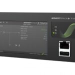
Advantage Controls H12 MegaTron Controller
 Manual
Megatron
Controller
Supplemental
Modbus H12 / H16 Communications Manual
- Advantage Controls
- 4700 Harold-Abitz Dr.
- Muskogee, OK 74403
- Phone: 800-743-7431
- Fax: 888-686-6212 www.advantagecontrols.com
- email: support@advantagecontrols.com
Modbus Introduction
The Advantage Controls MegaTron is capable of supporting TCP/IP communications via Ethernet and Data Modem. This allows for connections to our custom embedded web server via local networks and our browser based WebAdvantage service. Advantage Controls has now implemented Modbus/TCP support which allows interfacing with more customizable PC applications using HMI/SCADA and stand-alone HMI systems.
The MegaTron controller is capable of connecting to the WebAdvantage Server and most Building Management Systems. The WebAdvantage service requires a gateway to the internet with firewalls and security rules in place. The Building Management System needs to be on the same subnet to properly receive traffic from the MegaTron. This may require some advanced routing of network traffic within the network wiring or programming of advanced switching equipment. The datatraffic for both is provided via the same Ethernet cable coming from the MegaTron.
Modbus Overview
Modbus is a messaging protocol developed by Modicon in 1979. It’s used to establish a client-server communication between Modbus intelligent enabled devices. Modbus is a de facto standard open and widely used network protocol within industrial manufacturing environments. The protocol is used totransfer analog I/O and register data between Modbus enabled systems.
The Advantage Controls MegaTron utilizes Modbus/TCP protocol via an Ethernet handoff. Modbus is an application layer messaging protocol, located at level 7 of the OSI model providing client-server communications between devices positioned different types of buses or networks.
Addresses use one based numbering. For systems that use zero based numbering remove 1 (3001 becomes 3000 2002:12 becomes 2001:11) All address are read-only holding registers. Data is sent in little-endian byte order. If data does not appear correct in your system you can try byte swapping or word swapping. Communication card can talk to WebAdvantage and BMS/EMS systems at the same time. For registers size 2 values you must look at both values to get correct reading.
Note: To write to the Registers use Function Code 16.
* For more information about Modbus please visit www.modbus.org.
MegaTron Quick Steps
Connecting to MODBUS enabled MegaTron
This guide is designed to help with connecting a MODBUS enabled MegaTron to a local BMS.
Note: Screens may vary slightly between models.
MODBUS Setup
- Step 1:
Press Setup/Run, CONFIGURE, NETWORK, SETTINGS. (See figures 1, 2, 3 and 4. H15 dual cards add figure 3B. H15 only available for MegaTron MT.) - Step 2:
Press DHCP. (See figure 5.) Note: If these options are not visible, the dual network card needs to be enabled. See enabling dual network card to continue setup. - Step 3:
Use the up/down arrows to enable DHCP. Press Enter to accept. (See figure 6.) - Step 4:
Press RESET and then press Enter to accept. The communications card will reset after a short countdown. (See figures 7 and 8.) - Step 5:
After the communications card has been reset cycle power to the controller.


Modbus/TCP Data Dictionary – Rev. JA. 12.1
Data Types
| Data Types |
| Bit – 1-Bit (16 Bits per Register) |
| Float – 32-Bit Floating Point |
| Long – 32-Bit Integer |
| Short – 16-Bit Integer |
| String – 8-Bits (2 per Register) |
Controller Data
| Controller Data | Addr. | Reg.Qty. | Size | Type | Writeable |
| Name | 0001 | 16 | 32 | String | No |
| Serial Number | 0017 | 16 | 32 | String | No |
| Firmware Version | 0033 | 16 | 32 | String | No |
| Date | 0049 | 4 | 8 | String | No |
| Time | 0053 | 4 | 8 | String | No |
| Day of Week | 0057 | 1 | 1 | Short | No |
| Read-Only Mode | 0058 | 1 | 1 | Short | No |
Configuration Data
| Configuration Data | Addr. | Reg. Size | Qty. | Total | Type | Writeable |
| Conductivity – Set Pt #1 [1-4] | 1001 | 1 | 4 | 4 | Short | Yes |
| Conductivity – Set Pt #2 [1-4] | 1005 | 1 | 4 | 4 | Short | Yes |
| Conductivity – High Alarm Set Pt [1-4] | 1009 | 1 | 4 | 4 | Short | Yes |
| Conductivity – Low Alarm Set Pt [1-4] | 1013 | 1 | 4 | 4 | Short | Yes |
| Makeup Cond. – Set Pt #1 [1-4] | 1017 | 1 | 4 | 4 | Short | Yes |
| Makeup Cond. – High Alarm Set Pt [1-4] | 1021 | 1 | 4 | 4 | Short | Yes |
| Makeup Cond. – Low Alarm Set Pt [1-4] | 1025 | 1 | 4 | 4 | Short | Yes |
| pH – Set Pt #1 [1-4] | 1029 | 2 | 4 | 8 | Float | Yes |
| pH – Set Pt #2 [1-4] | 1037 | 2 | 4 | 8 | Float | Yes |
| pH – High Alarm Set Pt [1-4] | 1045 | 2 | 4 | 8 | Float | Yes |
| pH – Low Alarm Set Pt [1-4] | 1053 | 2 | 4 | 8 | Float | Yes |
| ORP – Set Pt #1 [1-4] | 1061 | 2 | 4 | 8 | Float | Yes |
| ORP – Set Pt #2 [1-4] | 1069 | 2 | 4 | 8 | Float | Yes |
| ORP – High Alarm Set Pt [1-4] | 1077 | 2 | 4 | 8 | Float | Yes |
| ORP – Low Alarm Set Pt [1-4] | 1085 | 2 | 4 | 8 | Float | Yes |
| System Temp. – Set Pt #1 [1-4] | 1093 | 2 | 4 | 8 | Float | Yes |
| System Temp. – High Alarm Set Pt [1-4] | 1101 | 2 | 4 | 8 | Float | Yes |
| System Temp. – Low Alarm Set Pt [1-4] | 1109 | 2 | 4 | 8 | Float | Yes |
| Auxiliary Temp. – Set Pt #1 [1-4] | 1117 | 2 | 4 | 8 | Float | Yes |
| Auxiliary Temp. – High Alarm Set Pt [1-4] | 1125 | 2 | 4 | 8 | Float | Yes |
| Auxiliary Temp. – Low Alarm Set Pt [1-4] | 1133 | 2 | 4 | 8 | Float | Yes |
| Delta Temp. – Set Pt #1 [1-4] | 1141 | 2 | 4 | 8 | Float | Yes |
| Delta Temp. – High Alarm Set Pt [1-4] | 1149 | 2 | 4 | 8 | Float | Yes |
| Delta Temp. – Low Alarm Set Pt [1-4] | 1157 | 2 | 4 | 8 | Float | Yes |
| Flow Switch – Configuration [1-4] | 1165 | 1 | 4 | 4 | Short | Yes |
| Temperature Scale | 1169 | 1 | 1 | 4 | Short | No |
| System 1 – Timer – Limit Time [1-5] | 1170 | 1 | 5 | 5 | Short | Yes |
| System 2 – Timer – Limit Time [1-5] | 1175 | 1 | 5 | 5 | Short | Yes |
| System 3 – Timer – Limit Time [1-5] | 1180 | 1 | 5 | 5 | Short | Yes |
| System 4 – Timer – Limit Time [1-5] | 1185 | 1 | 5 | 5 | Short | Yes |
Alarm Data
| Alarm Data | Address | Bit(s) | Type | Writeable |
| SYS1 HI COND | 2001:13 | 1 | Bit | No |
| SYS1 LOW COND | 2001:14 | 1 | Bit | No |
| SYS1 COND LIMIT | 2001:15 | 1 | Bit | No |
| SYS1 HI pH | 2001:16 | 1 | Bit | No |
| SYS1 LOW pH | 2002:1 | 1 | Bit | No |
| SYS1 ph LIMIT | 2002:2 | 1 | Bit | No |
| SYS1 HI ORP | 2002:3 | 1 | Bit | No |
| SYS1 LOW ORP | 2002:4 | 1 | Bit | No |
| SYS1 ORP LIMIT | 2002:5 | 1 | Bit | No |
| SYS1 HI TEMP 1 | 2002:6 | 1 | Bit | No |
| SYS1 LOW TEMP 1 | 2002:7 | 1 | Bit | No |
| SYS1 HI TEMP 2 | 2002:8 | 1 | Bit | No |
| SYS1 LOW TEMP 2 | 2002:9 | 1 | Bit | No |
| SYS1 HI DELTA TEMP | 2002:10 | 1 | Bit | No |
| SYS1 LOW DELTA TEMP | 2002:11 | 1 | Bit | No |
| SYS1 NO FLOW | 2002:12 | 1 | Bit | No |
| SYS1 DIGITAL INPUT 1 | 2002:13 | 1 | Bit | No |
| SYS1 DIGITAL INPUT 2 | 2002:14 | 1 | Bit | No |
| SYS1 DIGITAL INPUT 3 | 2002:15 | 1 | Bit | No |
| SYS1 DIGITAL INPUT 4 | 2002:16 | 1 | Bit | No |
| SYS1 DIGITAL INPUT 5 | 2003:1 | 1 | Bit | No |
| SYS1 HI MCND | 2003:3 | 1 | Bit | No |
| SYS1 LOW MCND | 2003:4 | 1 | Bit | No |
| SYS1 MCND LIMIT | 2003:5 | 1 | Bit | No |
| SYS1 NOTE 1 HI | 2003:6 | 1 | Bit | No |
| SYS1 NOTE 2 HI | 2003:7 | 1 | Bit | No |
| SYS1 NOTE 3 HI | 2003:8 | 1 | Bit | No |
| SYS1 NOTE 4 HI | 2003:9 | 1 | Bit | No |
| SYS1 NOTE 5 HI | 2003:10 | 1 | Bit | No |
| SYS1 NOTE 6 HI | 2003:11 | 1 | Bit | No |
| SYS1 NOTE 7 HI | 2003:12 | 1 | Bit | No |
| SYS1 NOTE 8 HI | 2003:13 | 1 | Bit | No |
| SYS1 NOTE 9 HI | 2003:14 | 1 | Bit | No |
| SYS1 NOTE 10 HI | 2003:15 | 1 | Bit | No |
| SYS1 NOTE 1 LOW | 2003:16 | 1 | Bit | No |
| SYS1 NOTE 2 LOW | 2004:1 | 1 | Bit | No |
| SYS1 NOTE 3 LOW | 2004:2 | 1 | Bit | No |
| SYS1 NOTE 4 LOW | 2004:3 | 1 | Bit | No |
| SYS1 NOTE 5 LOW | 2004:4 | 1 | Bit | No |
| SYS1 NOTE 6 LOW | 2004:5 | 1 | Bit | No |
| SYS1 NOTE 7 LOW | 2004:6 | 1 | Bit | No |
| SYS1 NOTE 8 LOW | 2004:7 | 1 | Bit | No |
| SYS1 NOTE 9 LOW | 2004:8 | 1 | Bit | No |
| SYS1 NOTE 10 LOW | 2004:9 | 1 | Bit | No |
| SYS1 NOTE 1 TIME | 2004:10 | 1 | Bit | No |
| SYS1 NOTE 2 TIME | 2004:11 | 1 | Bit | No |
| SYS1 NOTE 3 TIME | 2004:12 | 1 | Bit | No |
| SYS1 NOTE 4 TIME | 2004:13 | 1 | Bit | No |
| SYS1 NOTE 5 TIME | 2004:14 | 1 | Bit | No |
| SYS1 NOTE 6 TIME | 2004:15 | 1 | Bit | No |
| SYS1 NOTE 7 TIME | 2004:16 | 1 | Bit | No |
| SYS1 NOTE 8 TIME | 2005:1 | 1 | Bit | No |
| SYS1 NOTE 9 TIME | 2005:2 | 1 | Bit | No |
| SYS1 NOTE 10 TIME | 2005:3 | 1 | Bit | No |
| SYS2 HI COND | 2008:13 | 1 | Bit | No |
| SYS2 LOW COND | 2008:14 | 1 | Bit | No |
| SYS2 COND LIMIT | 2008:15 | 1 | Bit | No |
| SYS2 HI ph | 2008:16 | 1 | Bit | No |
| SYS2 LOW ph | 2009:1 | 1 | Bit | No |
| SYS2 ph LIMIT | 2009:2 | 1 | Bit | No |
| SYS2 HI ORP | 2009:3 | 1 | Bit | No |
| SYS2 LOW ORP | 2009:4 | 1 | Bit | No |
| SYS2 ORP LIMIT | 2009:5 | 1 | Bit | No |
| SYS2 HI TEMP 1 | 2009:6 | 1 | Bit | No |
| SYS2 LOW TEMP 1 | 2009:7 | 1 | Bit | No |
| SYS2 HI TEMP 2 | 2009:8 | 1 | Bit | No |
| SYS2 LOW TEMP 2 | 2009:9 | 1 | Bit | No |
| SYS2 HI DELTA TEMP | 2009:10 | 1 | Bit | No |
| SYS2 LOW DELTA TEMP | 2009:11 | 1 | Bit | No |
| SYS2 NO FLOW | 2009:12 | 1 | Bit | No |
| SYS2 DIGITAL INPUT 1 | 2009:13 | 1 | Bit | No |
| SYS2 DIGITAL INPUT 2 | 2009:14 | 1 | Bit | No |
| SYS2 DIGITAL INPUT 3 | 2009:15 | 1 | Bit | No |
| SYS2 DIGITAL INPUT 4 | 2009:16 | 1 | Bit | No |
| SYS2 DIGITAL INPUT 5 | 2010:1 | 1 | Bit | No |
| SYS2 HI MCND | 2010:3 | 1 | Bit | No |
| SYS2 LOW MCND | 2010:4 | 1 | Bit | No |
| SYS2 MCND LIMIT | 2010:5 | 1 | Bit | No |
| SYS2 NOTE 1 HI | 2010:6 | 1 | Bit | No |
| SYS2 NOTE 2 HI | 2010:7 | 1 | Bit | No |
| SYS2 NOTE 3 HI | 2010:8 | 1 | Bit | No |
| SYS2 NOTE 4 HI | 2010:9 | 1 | Bit | No |
| SYS2 NOTE 5 HI | 2010:10 | 1 | Bit | No |
| SYS2 NOTE 6 HI | 2010:11 | 1 | Bit | No |
| SYS2 NOTE 7 HI | 2010:12 | 1 | Bit | No |
| SYS2 NOTE 8 HI | 2010:13 | 1 | Bit | No |
| SYS2 NOTE 9 HI | 2010:14 | 1 | Bit | No |
| SYS2 NOTE 10 HI | 2010:15 | 1 | Bit | No |
| SYS2 NOTE 1 LOW | 2010:16 | 1 | Bit | No |
| SYS2 NOTE 2 LOW | 2011:1 | 1 | Bit | No |
| SYS2 NOTE 3 LOW | 2011:2 | 1 | Bit | No |
| SYS2 NOTE 4 LOW | 2011:3 | 1 | Bit | No |
| SYS2 NOTE 5 LOW | 2011:4 | 1 | Bit | No |
| SYS2 NOTE 6 LOW | 2011:5 | 1 | Bit | No |
| SYS2 NOTE 7 LOW | 2011:6 | 1 | Bit | No |
| SYS2 NOTE 8 LOW | 2011:7 | 1 | Bit | No |
| SYS2 NOTE 9 LOW | 2011:8 | 1 | Bit | No |
| SYS2 NOTE 10 LOW | 2011:9 | 1 | Bit | No |
| SYS2 NOTE 1 TIME | 2011:10 | 1 | Bit | No |
| SYS2 NOTE 2 TIME | 2011:11 | 1 | Bit | No |
| SYS2 NOTE 3 TIME | 2011:12 | 1 | Bit | No |
| SYS2 NOTE 4 TIME | 2011:13 | 1 | Bit | No |
| SYS2 NOTE 5 TIME | 2011:14 | 1 | Bit | No |
| SYS2 NOTE 6 TIME | 2011:15 | 1 | Bit | No |
| SYS2 NOTE 7 TIME | 2011:16 | 1 | Bit | No |
| SYS2 NOTE 8 TIME | 2012:1 | 1 | Bit | No |
| SYS2 NOTE 9 TIME | 2012:2 | 1 | Bit | No |
| SYS2 NOTE 10 TIME | 2012:3 | 1 | Bit | No |
| SYS3 HI COND | 2015:13 | 1 | Bit | No |
| SYS3 LOW COND | 2015:14 | 1 | Bit | No |
| SYS3 COND LIMIT | 2015:15 | 1 | Bit | No |
| SYS3 HI pH | 2015:16 | 1 | Bit | No |
| SYS3 LOW pH | 2016:1 | 1 | Bit | No |
| SYS3 pH LIMIT | 2016:2 | 1 | Bit | No |
| SYS3 HI ORP | 2016:3 | 1 | Bit | No |
| SYS3 LOW ORP | 2016:4 | 1 | Bit | No |
| SYS3 ORP LIMIT | 2016:5 | 1 | Bit | No |
| SYS3 HI TEMP 1 | 2016:6 | 1 | Bit | No |
| SYS3 LOW TEMP 1 | 2016:7 | 1 | Bit | No |
| SYS3 HI TEMP 2 | 2016:8 | 1 | Bit | No |
| SYS3 LOW TEMP 2 | 2016:9 | 1 | Bit | No |
| SYS3 HI DELTA TEMP | 2016:10 | 1 | Bit | No |
| SYS3 LOW DELTA TEMP | 2016:11 | 1 | Bit | No |
| SYS3 NO FLOW | 2016:12 | 1 | Bit | No |
| SYS3 DIGITAL INPUT 1 | 2016:13 | 1 | Bit | No |
| SYS3 DIGITAL INPUT 2 | 2016:14 | 1 | Bit | No |
| SYS3 DIGITAL INPUT 3 | 2016:15 | 1 | Bit | No |
| SYS3 DIGITAL INPUT 4 | 2016:16 | 1 | Bit | No |
| SYS3 DIGITAL INPUT 5 | 2017:1 | 1 | Bit | No |
| SYS3 HI MCND | 2017:3 | 1 | Bit | No |
| SYS3 LOW MCND | 2017:4 | 1 | Bit | No |
| SYS3 MCND LIMIT | 2017:5 | 1 | Bit | No |
| SYS3 NOTE 1 HI | 2017:6 | 1 | Bit | No |
| SYS3 NOTE 2 HI | 2017:7 | 1 | Bit | No |
| SYS3 NOTE 3 HI | 2017:8 | 1 | Bit | No |
| SYS3 NOTE 4 HI | 2017:9 | 1 | Bit | No |
| SYS3 NOTE 5 HI | 2017:10 | 1 | Bit | No |
| SYS3 NOTE 6 HI | 2017:11 | 1 | Bit | No |
| SYS3 NOTE 7 HI | 2017:12 | 1 | Bit | No |
| SYS3 NOTE 8 HI | 2017:13 | 1 | Bit | No |
| SYS3 NOTE 9 HI | 2017:14 | 1 | Bit | No |
| SYS3 NOTE 10 HI | 2017:15 | 1 | Bit | No |
| SYS3 NOTE 1 LOW | 2017:16 | 1 | Bit | No |
| SYS3 NOTE 2 LOW | 2018:1 | 1 | Bit | No |
| SYS3 NOTE 3 LOW | 2018:2 | 1 | Bit | No |
| SYS3 NOTE 4 LOW | 2018:3 | 1 | Bit | No |
| SYS3 NOTE 5 LOW | 2018:4 | 1 | Bit | No |
| SYS3 NOTE 6 LOW | 2018:5 | 1 | Bit | No |
| SYS3 NOTE 7 LOW | 2018:6 | 1 | Bit | No |
| SYS3 NOTE 8 LOW | 2018:7 | 1 | Bit | No |
| SYS3 NOTE 9 LOW | 2018:8 | 1 | Bit | No |
| SYS3 NOTE 10 LOW | 2018:9 | 1 | Bit | No |
| SYS3 NOTE 1 TIME | 2018:10 | 1 | Bit | No |
| SYS3 NOTE 2 TIME | 2018:11 | 1 | Bit | No |
| SYS3 NOTE 3 TIME | 2018:12 | 1 | Bit | No |
| SYS3 NOTE 4 TIME | 2018:13 | 1 | Bit | No |
| SYS3 NOTE 5 TIME | 2018:14 | 1 | Bit | No |
| SYS3 NOTE 6 TIME | 2018:15 | 1 | Bit | No |
| SYS3 NOTE 7 TIME | 2018:16 | 1 | Bit | No |
| SYS3 NOTE 8 TIME | 2019:1 | 1 | Bit | No |
| SYS3 NOTE 9 TIME | 2019:2 | 1 | Bit | No |
| SYS3 NOTE 10 TIME | 2019:3 | 1 | Bit | No |
| SYS4 HI COND | 2022:13 | 1 | Bit | No |
| SYS4 LOW COND | 2022:14 | 1 | Bit | No |
| SYS4 COND LIMIT | 2022:15 | 1 | Bit | No |
| SYS4 HI ph | 2022:16 | 1 | Bit | No |
| SYS4 LOW ph | 2023:1 | 1 | Bit | No |
| SYS4 ph LIMIT | 2023:2 | 1 | Bit | No |
| SYS4 HI ORP | 2023:3 | 1 | Bit | No |
| SYS4 LOW ORP | 2023:4 | 1 | Bit | No |
| SYS4 ORP LIMIT | 2023:5 | 1 | Bit | No |
| SYS4 HI TEMP 1 | 2023:6 | 1 | Bit | No |
| SYS4 LOW TEMP 1 | 2023:7 | 1 | Bit | No |
| SYS4 HI TEMP 2 | 2023:8 | 1 | Bit | No |
| SYS4 LOW TEMP 2 | 2023:9 | 1 | Bit | No |
| SYS4 HI DELTA TEMP | 2023:10 | 1 | Bit | No |
| SYS4 LOW DELTA TEMP | 2023:11 | 1 | Bit | No |
| SYS4 NO FLOW | 2023:12 | 1 | Bit | No |
| SYS4 DIGITAL INPUT 1 | 2023:13 | 1 | Bit | No |
| SYS4 DIGITAL INPUT 2 | 2023:14 | 1 | Bit | No |
| SYS4 DIGITAL INPUT 3 | 2023:15 | 1 | Bit | No |
| SYS4 DIGITAL INPUT 4 | 2023:16 | 1 | Bit | No |
| SYS4 DIGITAL INPUT 5 | 2024:1 | 1 | Bit | No |
| SYS4 HI MCND | 2024:3 | 1 | Bit | No |
| SYS4 LOW MCND | 2024:4 | 1 | Bit | No |
| SYS4 MCND LIMIT | 2024:5 | 1 | Bit | No |
| SYS4 NOTE 1 HI | 2024:6 | 1 | Bit | No |
| SYS4 NOTE 2 HI | 2024:7 | 1 | Bit | No |
| SYS4 NOTE 3 HI | 2024:8 | 1 | Bit | No |
| SYS4 NOTE 4 HI | 2024:9 | 1 | Bit | No |
| SYS4 NOTE 5 HI | 2024:10 | 1 | Bit | No |
| SYS4 NOTE 6 HI | 2024:11 | 1 | Bit | No |
| SYS4 NOTE 7 HI | 2024:12 | 1 | Bit | No |
| SYS4 NOTE 8 HI | 2024:13 | 1 | Bit | No |
| SYS4 NOTE 9 HI | 2024:14 | 1 | Bit | No |
| SYS4 NOTE 10 HI | 2024:15 | 1 | Bit | No |
| SYS4 NOTE 1 LOW | 2024:16 | 1 | Bit | No |
| SYS4 NOTE 2 LOW | 2025:1 | 1 | Bit | No |
| SYS4 NOTE 3 LOW | 2025:2 | 1 | Bit | No |
| SYS4 NOTE 4 LOW | 2025:3 | 1 | Bit | No |
| SYS4 NOTE 5 LOW | 2025:4 | 1 | Bit | No |
| SYS4 NOTE 6 LOW | 2025:5 | 1 | Bit | No |
| SYS4 NOTE 7 LOW | 2025:6 | 1 | Bit | No |
| SYS4 NOTE 8 LOW | 2025:7 | 1 | Bit | No |
| SYS4 NOTE 9 LOW | 2025:8 | 1 | Bit | No |
| SYS4 NOTE 10 LOW | 2025:9 | 1 | Bit | No |
| SYS4 NOTE 1 TIME | 2025:10 | 1 | Bit | No |
| SYS4 NOTE 2 TIME | 2025:11 | 1 | Bit | No |
| SYS4 NOTE 3 TIME | 2025:12 | 1 | Bit | No |
| SYS4 NOTE 4 TIME | 2025:13 | 1 | Bit | No |
| SYS4 NOTE 5 TIME | 2025:14 | 1 | Bit | No |
| SYS4 NOTE 6 TIME | 2025:15 | 1 | Bit | No |
| SYS4 NOTE 7 TIME | 2025:16 | 1 | Bit | No |
| SYS4 NOTE 8 TIME | 2026:1 | 1 | Bit | No |
| SYS4 NOTE 9 TIME | 2026:2 | 1 | Bit | No |
| SYS4 NOTE 10 TIME | 2026:3 | 1 | Bit | No |
| MA IN1 HIGH | 2029:2 | 1 | Bit | No |
| MA IN1 LOW | 2029:3 | 1 | Bit | No |
| MA IN2 HIGH | 2029:5 | 1 | Bit | No |
| MA IN2 LOW | 2029:6 | 1 | Bit | No |
| MA IN3 HIGH | 2029:8 | 1 | Bit | No |
| MA IN3 LOW | 2029:9 | 1 | Bit | No |
| MA IN4 HIGH | 2029:11 | 1 | Bit | No |
| MA IN4 LOW | 2029:12 | 1 | Bit | No |
| MA IN5 HIGH | 2029:14 | 1 | Bit | No |
| MA IN5 LOW | 2029:15 | 1 | Bit | No |
| MA IN6 HIGH | 2030:1 | 1 | Bit | No |
| MA IN6 LOW | 2030:2 | 1 | Bit | No |
| MA IN7 HIGH | 2030:4 | 1 | Bit | No |
| MA IN7 LOW | 2030:5 | 1 | Bit | No |
| MA IN8 HIGH | 2030:7 | 1 | Bit | No |
| MA IN8 LOW | 2030:8 | 1 | Bit | No |
| FM1 FLOW | 2030:11 | 1 | Bit | No |
| FM1 FLOW VERIFY | 2030:12 | 1 | Bit | No |
| FM1 VOLUME | 2030:13 | 1 | Bit | No |
| FM2 FLOW | 2030:14 | 1 | Bit | No |
| FM2 FLOW VERIFY | 2030:15 | 1 | Bit | No |
| FM2 VOLUME | 2030:16 | 1 | Bit | No |
| FM3 FLOW | 2031:1 | 1 | Bit | No |
| FM3 FLOW VERIFY | 2031:2 | 1 | Bit | No |
| FM3 VOLUME | 2031:3 | 1 | Bit | No |
| FM4 FLOW | 2031:4 | 1 | Bit | No |
| FM4 FLOW VERIFY | 2031:5 | 1 | Bit | No |
| FM4 VOLUME | 2031:6 | 1 | Bit | No |
| FM5 FLOW | 2031:7 | 1 | Bit | No |
| FM5 FLOW VERIFY | 2031:8 | 1 | Bit | No |
| FM5 VOLUME | 2031:9 | 1 | Bit | No |
| FM6 FLOW | 2031:10 | 1 | Bit | No |
| FM6 FLOW VERIFY | 2031:11 | 1 | Bit | No |
| FM6 VOLUME | 2031:12 | 1 | Bit | No |
| FM7 FLOW | 2031:13 | 1 | Bit | No |
| FM7 FLOW VERIFY | 2031:14 | 1 | Bit | No |
| FM7 VOLUME | 2031:15 | 1 | Bit | No |
| FM8 FLOW | 2031:16 | 1 | Bit | No |
| FM8 FLOW VERIFY | 2032:1 | 1 | Bit | No |
| FM8 VOLUME | 2032:2 | 1 | Bit | No |
| FM9 FLOW | 2032:3 | 1 | Bit | No |
| FM9 FLOW VERIFY | 2032:4 | 1 | Bit | No |
| FM9 VOLUME | 2032:5 | 1 | Bit | No |
| FM10 FLOW | 2032:6 | 1 | Bit | No |
| FM10 FLOW VERIFY | 2032:7 | 1 | Bit | No |
| FM10 VOLUME | 2032:8 | 1 | Bit | No |
| R1 MAX HRS | 2032:9 | 1 | Bit | No |
| R2 MAX HRS | 2032:10 | 1 | Bit | No |
| R3 MAX HRS | 2032:11 | 1 | Bit | No |
| R4 MAX HRS | 2032:12 | 1 | Bit | No |
| R5 MAX HRS | 2032:13 | 1 | Bit | No |
| R6 MAX HRS | 2032:14 | 1 | Bit | No |
| R7 MAX HRS | 2032:15 | 1 | Bit | No |
| R8 MAX HRS | 2032:16 | 1 | Bit | No |
| R9 MAX HRS | 2033:1 | 1 | Bit | No |
| R10 MAX HRS | 2033:2 | 1 | Bit | No |
| R11 MAX HRS | 2033:3 | 1 | Bit | No |
| R12 MAX HRS | 2033:4 | 1 | Bit | No |
| R13 MAX HRS | 2033:5 | 1 | Bit | No |
| R14 MAX HRS | 2033:6 | 1 | Bit | No |
| R15 MAX HRS | 2033:7 | 1 | Bit | No |
| R16 MAX HRS | 2033:8 | 1 | Bit | No |
| R17 MAX HRS | 2033:9 | 1 | Bit | No |
| R18 MAX HRS | 2033:10 | 1 | Bit | No |
| R19 MAX HRS | 2033:11 | 1 | Bit | No |
| R20 MAX HRS | 2033:12 | 1 | Bit | No |
| MA IN1 LIMIT | 2033:13 | 1 | Bit | No |
| MA IN2 LIMIT | 2033:14 | 1 | Bit | No |
| MA IN3 LIMIT | 2033:15 | 1 | Bit | No |
| MA IN4 LIMIT | 2033:16 | 1 | Bit | No |
| MA IN5 LIMIT | 2034:1 | 1 | Bit | No |
| MA IN6 LIMIT | 2034:2 | 1 | Bit | No |
| MA IN7 LIMIT | 2034:3 | 1 | Bit | No |
| MA IN8 LIMIT | 2034:4 | 1 | Bit | No |
| MA IN9 LIMIT | 2034:5 | 1 | Bit | No |
| MA IN10 LIMIT | 2034:6 | 1 | Bit | No |
| MA IN11 LIMIT | 2034:7 | 1 | Bit | No |
| MA IN12 LIMIT | 2034:8 | 1 | Bit | No |
| MA IN13 LIMIT | 2034:9 | 1 | Bit | No |
| MA IN14 LIMIT | 2034:10 | 1 | Bit | No |
| MA IN15 LIMIT | 2034:11 | 1 | Bit | No |
| MA IN16 LIMIT | 2034:12 | 1 | Bit | No |
| MA IN9 HIGH | 2034:14 | 1 | Bit | No |
| MA IN9 LOW | 2034:15 | 1 | Bit | No |
| MA IN10 HIGH | 2035:1 | 1 | Bit | No |
| MA IN10 LOW | 2035:2 | 1 | Bit | No |
| MA IN11HIGH | 2035:4 | 1 | Bit | No |
| MA IN11 LOW | 2035:5 | 1 | Bit | No |
| MA IN12 HIGH | 2035:7 | 1 | Bit | No |
| MA IN12 LOW | 2035:8 | 1 | Bit | No |
| MA IN13 HIGH | 2035:10 | 1 | Bit | No |
| MA IN13 LOW | 2035:11 | 1 | Bit | No |
| MA IN14 HIGH | 2035:13 | 1 | Bit | No |
| MA IN14 LOW | 2035:14 | 1 | Bit | No |
| MA IN15 HIGH | 2035:16 | 1 | Bit | No |
| MA IN15 LOW | 2036:1 | 1 | Bit | No |
| MA IN16 HIGH | 2036:3 | 1 | Bit | No |
| MA IN16 LOW | 2036:4 | 1 | Bit | No |
Sensor Data
| Sensor Data | Addr. | Reg. Size | Qty. | Total | Type | Writeable |
| Conductivity [1-4] | 3001 | 1 | 4 | 4 | Short | No |
| Makeup Cond. [1-4] | 3005 | 1 | 4 | 4 | Short | No |
| pH [1-4] | 3009 | 2 | 4 | 8 | Float | No |
| ORP [1-4] | 3017 | 2 | 4 | 8 | Float | No |
| System Temp. [1-4] | 3025 | 2 | 4 | 8 | Float | No |
| Auxiliary Temp. [1-4] | 3033 | 2 | 4 | 8 | Float | No |
| Flow [1-4] | 3041 | 1 | 4 | 4 | Short | No |
| Water Meter #1 – Total Value [1-4] | 3045 | 2 | 4 | 8 | Long | No |
| Water Meter #2 – Total Value [1-4] | 3053 | 2 | 4 | 8 | Long | No |
| Makeup Cycles [1-4] | 3061 | 2 | 4 | 8 | Float | No |
Relay Data
| Relay Data | Addr. | Reg. Size | Qty. | Total | Type | Writeable |
| Relay [1-20] ( See Note #1) | 4001 | 1 | 20 | 20 | Short | Yes |
Note #1 0=H-OFF 1=H-ON 2=OFF 3=ON
mA Output Data
| mA Output Data | Addr. | Reg. Size | Qty. | Total | Type | Writeable |
| Value [1-6] | 4201 | 2 | 6 | 12 | Float | No |
4-20mA / 0-5V Input Data
| 4-20mA / 0-5V Input Data | Addr. | Reg. Size | Qty. | Total | Type | Writeable |
| Value [1-16] | 4251 | 2 | 16 | 32 | Float | No |
Flow Meter Data
| Flow Meter Data | Addr. | Reg. Size | Qty. | Total | Type | Writeable |
| Total [1-10] | 4301 | 2 | 10 | 20 | Float | No |
| Flow Rate [1-10] | 4321 | 2 | 10 | 20 | Float | No |
Get the Advantage in Water Treatment Equipment
Advantage Controls can give you the Advantage in products, knowledge and support on all of your water treatment equipment needs.
- Cooling Tower Controllers
- Boiler Blow Down Controllers
- Blow Down Valve Packages
- Solenoid Valves
- Water Meters
- Chemical Metering Pumps
- Corrosion Coupon Racks
- Chemical Solution Tanks
- Solid Feed Systems
- Feed Timers
- Filter Equipment
- Glycol Feed Systems
- Pre Fabricated Systems


 Get the Advantage
Documents / Resources
 |
Advantage Controls H12 MegaTron Controller [pdf] Owner's Manual H12, H12 MegaTron Controller, MegaTron Controller, Controller |