![]() life.augmented
life.augmented
UM2154
User manual
STEVE-SPIN3201: advanced BLDC controller with embedded STM32 MCU evaluation board
Introduction
The STEVAL-SPIN3201 board is a 3-phase brushless DC motor driver board based on the STSPIN32F0, a 3-phase controller with an integrated STM32 MCU, and implements 3-shunt resistors as current reading topology.
It provides an easy-to-use solution for the evaluation of the device in different applications such as the home appliance, fans, drones, and power tools.
The board is designed for the sensored or sensorless field-oriented control algorithm with 3-shunt sensing.
Figure 1. STEVE-SPIN3201 evaluation board

Hardware and software requirements
Using the STEVAL-SPIN3201 evaluation board requires the following software and hardware:
- A Windows ® PC (XP, Vista 7, Windows 8, Windows 10) to install the software package
- A mini-B USB cable to connect the STEVAL-SPIN3201 board to the PC
- The STM32 Motor Control Software Development Kit Rev Y (X-CUBE-MCSDK-Y)
- A 3-phase brushless DC motor with a compatible voltage and current ratings
- An external DC power supply.
Getting started
The maximum ratings of the board are the following:
- Power stage supply voltage (VS) from 8 V to 45 V
- Motor phase current up to 15 Arms
To start your project with the board:
Step 1. Check the jumper position according to the target configuration (see Section 4.3 Overcurrent detection
Step 2. Connect the motor to the connector J3 taking care of the sequence of the motor phases.
Step 3. Supply the board through the input 1 and 2 of the connector J2. The DL1 (red) LED will turn on.
Step 4. Develop your application using the STM32 Motor Control Software Development Kit Rev Y (X-CUBEMCSDK-Y).
Hardware description and configuration
Figure 2. Main components and connectors’ positions show the position of the main components and connectors on the board.
Figure 2. Main components and connectors positions

Table 1. Hardware setting jumpers provide the detailed pinout of the connectors.
Table 1. Hardware setting jumpers
| Jumper | Permitted configurations | Default condition |
| JP1 | Selection of VREG connected to V motor | OPEN |
| JP2 | Selection motor power supply connected to DC power supply | CLOSED |
| JP3 | Selection Hall encoder supply to USB (1) / VDD (3) power supply | 1 – 2 CLOSED |
| JP4 | Selection reset of ST-LINK (U4) | OPEN |
| JP5 | Selection PA2 connected to Hall 3 | CLOSED |
| JP6 | Selection PA1 connected to Hall 2 | CLOSED |
| JP7 | Selection PA0 connected to Hall 1 | CLOSED |
Table 2. Other connectors, jumper, and test points description
|
Name |
Pin | Label |
Description |
| J1 | 1 – 2 | J1 | Motor power supply |
| J2 | 1 – 2 | J2 | Device main power supply (VM) |
| J3 | 1 – 2 – 3 | U, V, W | 3-phase BLDC motor phases connection |
| J4 | 1 – 2 – 3 | J4 | Hall/encoder sensors connector |
| 4 – 5 | J4 | Hall sensors/encoder supply | |
| J5 | – | J5 | USB input ST-LINK |
| J6 | 1 | 3V3 | ST-LINK power supply |
| 2 | CLK | SWCLK of ST-LINK | |
| 3 | GND | GND | |
| 4 | DIO | SWDIO of ST-LINK | |
| J7 | 1 – 2 | J7 | CART |
| J8 | 1 – 2 | J8 | ST-LINK reset |
| TP1 | – | GREG | 12 V voltage regulator output |
| TP2 | – | GND | GND |
| TP3 | – | VDD | VDD |
| TP4 | – | SPEED | Speed potentiometer output |
| TP5 | – | PA3 | PA3 GPIO (output op-amp sense 1) |
| TP6 | – | VBUS | VBus feedback |
| TP7 | – | OUT_U | Output U |
| TP8 | – | PA4 | PA4 GPIO (output op-amp sense 2) |
| TP9 | – | PA5 | PA5 GPIO (output op-amp sense 3) |
| TP10 | – | GND | GND |
| TP11 | – | OUT_V | Output V |
| TP12 | – | PA7 | PA7_3FG |
| TP13 | – | OUT_W | Output W |
| TP14 | – | 3V3 | 3V3 ST-LINK |
| TP15 | – | 5V | USB voltage |
| TP16 | – | I/O | SWD_IO |
| TP17 | – | CLK | SWD_CLK |
Circuit description
The STEVAL-SPIN3201 provides a complete 3-shunt FOC solution composed of a STSPIN32F0 – advanced BLDC controller with an embedded STM32 MCU – and a triple half-bridge power stage with the NMOS STD140N6F7.
The STSPIN32F0 autonomously generates all the required supply voltages: the internal DC/DC buck converter provides 3V3 and an internal linear regulator provides 12 V for the gate drivers.
The current feedback signal conditioning is performed through three of the operational amplifiers embedded into the device and an internal comparator performs overcurrent protection from shunt resistors.
Two user buttons, two LEDs, and a trimmer are available to implement simple user interfaces (e.g., starting/ stopping the motor and setting target speed).
The STEVAL-SPIN3201 board supports the quadrature encoder and digital Hall sensors as motor position feedback.
The board includes an ST-LINK-V2 allowing the user to debug and download firmware without any extra hardware tool.
4.1 Hall/encoder motor speed sensor
The STEVAL-SPIN3201 evaluation board supports the digital Hall and quadrature encoder sensors as motor position feedback.
The sensors can be connected to the STSPIN32F0 through the J4 connector is listed in
Table 3. Hall/encoder connector (J4).
| Name | Pin | Description |
| Hall1/A+ | 1 | Hall sensor 1/encoder out A+ |
| Hall2/B+ | 2 | Hall sensor 2/encoder out B+ |
| Hall3/Z+ | 3 | Hall sensor 3/encoder zero feedback |
| VDD sensor | 4 | Sensor supply voltage |
| GND | 5 | Ground |
A protection series resistor of 1 kΩ is mounted in a series with sensor outputs.
For sensors requiring an external pull-up, three 10 kΩ resistors are already mounted on the output lines and connected to the VDD voltage. On the same lines, a footprint for pull-down resistors is also available.
The jumper JP3 selects the power supply for the sensor supply voltage:
- Jumper between the pin 1 – pin 2: Hall sensors powered by VUSB (5 V)
- Jumper between the pin 1 – pin 2: Hall sensors powered by VDD (3.3 V)
The user can disconnect sensor outputs from the MCU GPIO opening jumpers JP5, JP6, and JP7.
4.2 Current sensing
In the STEVAL-SPIN3201 board, the current sensing signal conditioning is performed through three of the operational amplifiers embedded into the STSPIN32F0 device.
In a typical FOC application, the currents in the three half-bridges are sensed using a shunt resistor on the source of each low side power switch. The sense voltage signals are provided to an analog-to-digital converter in order to perform the matrix calculation related to a certain control technique. Those sense signals are usually shifted and amplified by dedicated op-amps in order to exploit the full range of the ADC (refer to Figure 3. Current sensing scheme example).
Figure 3. Current sensing scheme example

The sense signals have to be shifted and centered on VDD/2 voltage (about 1.65 V) and amplified again which provides the matching between the maximum value of the sensed signal and the full-scale range of the ADC.
The voltage shifting stage introduces attenuation (1/Gp) of the feedback signal which, together with the gain of the non-inverting configuration (Gn, fixed by Rn and Rf), contributes to the overall gain (G). As already mentioned, the goal is to establish the overall amplification network gain (G) so that the voltage on the shunt resistor corresponding to the maximum motor allowed current (ISmax peak value of motor rated current) fits the range of voltages readable by the ADC.

Note that, once G is fixed, it is better to configure it by lowering the initial attenuation 1/Gp as much as possible and, therefore the gain Gn. This is important not only to maximize the signal by the noise ratio but also to reduce the effect of the op-amp intrinsic offset on the output (proportional to Gn).
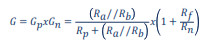
The gain and the polarization voltage (VOPout, pol) determine the operative range of the current sensing circuitry:
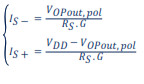 Where:
- IS- = maximum sourced current
- IS+ = maximum sunk current that can be sensed by the circuitry.
Table 4. STEVE-SPIN3201 op-amps polarization network
|
Parameter |
Part reference | Rev. 1 |
Rev. 3 |
| Rp | R14, R24, R33 | 560 Ω | 1.78 kΩ |
| Ra | R12, R20, R29 | 8.2 kΩ | 27.4 kΩ |
| Rb | R15, R25, R34 | 560 Ω | 27.4 kΩ |
| Rn | R13, R21, R30 | 1 kΩ | 1.78 kΩ |
| Rf | R9, R19, R28 | 15 kΩ | 13.7 kΩ |
| Cf | C15, C19, C20 | 100 pF | N. M. |
| G | – | 7.74 | 7.70 |
| VOPout, pol | – | 1.74 V | 1.65 V |
4.3 Overcurrent detection
The STEVAL-SPIN3201 evaluation board implements overcurrent protection based on the STSPIN32F0 integrated OC comparator. Shunt resistors measure the load current of each phase. The resistors R50, R51, and R52 bring the voltage signals associated with each load current to the OC_COMP pin. When the peak current flowing in one of the three phases exceeds the selected threshold, the integrated comparator is triggered and all the high side power switches are disabled. High-side power switches are enabled again when the current falls below the threshold, thus implementing overcurrent protection.
Current thresholds for the STEVAL-SPIN3201 evaluation board are listed in
Table 5. Overcurrent thresholds.
| PF6 | PF7 | Internal comp. threshold | OC threshold |
| 0 | 1 | 100 mV | 20 A |
| 1 | 0 | 250 mV | 65 A |
| 1 | 1 | 500 mV | 140 A |
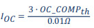
These thresholds can be modified by changing the R43 bias resistor. It is recommended to choose R43 higher than 30 kΩ. In order to calculate the value of the R43 for a target current limit IOC, the following formula can be used:
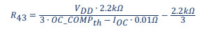
where OC_COMPth is the voltage threshold of the internal comparator (selected by the PF6 and PF7), and VDD is the 3.3 V digital supply voltage provided by the internal DCDC buck converter.
Removing the R43, the current threshold formula is simplified as follows:
4.4 Bus voltage circuit
The STEVAL-SPIN3201 evaluation board provides the bus voltage sensing. This signal is sent through a voltage divider from the motor supply voltage (VBUS) (R10 and R16) and sent to the PB1 GPIO (channel 9 of the ADC) of the embedded MCU. The signal is also available on the TP6.
4.5 Hardware user interface
The board includes the following hardware user interface items:
- Potentiometer R6: sets the target speed, for example
- Switch SW1: resets STSPIN32F0 MCU and ST-LINK V2
- Switch SW2: user button 1
- Switch SW3: user button 2
- LED DL3: user LED 1 (also turns on when user 1 button is pressed)
- LED DL4: user LED 2 (also turns on when user 2 buttons are pressed)
4.6 Debug
The STEVAL-SPIN3201 evaluation board embeds an ST-LINK/V2-1 debugger/programmer. The features supported on the ST-LINK are:
- USB software re-enumeration
- Virtual com port interface on USB connected to PB6/PB7 pins of the STSPIN32F0 (UART1)
- Mass storage interface on USB
The power supply for the ST-LINK is provided by the host PC through the USB cable connected to the J5.
The LED LD2 provides ST-LINK communication status information: - Red LED flashing slowly: at power-on before USB initialization
- Red LED flashing quickly: following first correct communication between the PC and ST-LINK/V2-1 (enumeration)
- Red LED ON: initialization between the PC and ST-LINK/V2-1 is complete
- Green LED ON: successful target communication initialization
- Red/green LED flashing: during communication with the target
- Green ON: communication finished and successful
The reset function is disconnected from the ST-LINK by removing the jumper J8.
Revision history
Table 6. Document revision history
| Date | Revision | Changes |
| 12-Dec-20161 | 1 | Initial release. |
| 23-Nov-2017 | 2 | Added Section 4.2: Current sensing on page 7. |
| 27-Feb-2018 | 3 | Minor modifications throughout the document. |
| 18-Aug-2021 | 4 | Minor template correction. |
STMicroelectronics NV and its subsidiaries (“ST”) reserve the right to make changes, corrections, enhancements, modifications, and improvements to ST products and/or to this document at any time without notice. Purchasers should obtain the latest relevant information on ST products before placing orders. ST products are sold pursuant to ST’s terms and conditions of sale in place at the time of order acknowledgment. Purchasers are solely responsible for the choice, selection, and use of ST products and ST assumes no liability for application assistance or the design of Purchasers’ products.
IMPORTANT NOTICE – PLEASE READ CAREFULLY
No license, express or implied, to any intellectual property right is granted by ST herein.
Resale of ST products with provisions different from the information set forth herein shall void any warranty granted by ST for such product.
ST and the ST logo are trademarks of ST. For additional information about ST trademarks, please refer to www.st.com/trademarks. All other product or service names are the property of their respective owners.
Information in this document supersedes and replaces information previously supplied in any prior versions of this document.
© 2021 STMicroelectronics – All rights reserved
Documents / Resources
 |
ST UM2154 STEVAL-SPIN3201 Advanced BLDC Controller with Embedded STM32 MCU Evaluation Board [pdf] User Manual UM2154, STEVAL-SPIN3201 Advanced BLDC Controller with Embedded STM32 MCU Evaluation Board |


