![]()
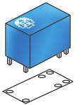
KA05
ILLUSTRATED ASSEMBLY MANUAL HKA05P’1
IN/OUT shield for Arduino®

General-purpose INPUT-OUTPUT shield for Arduino®
Features
- For use with Arduino Due, Arduino Uno, Arduino Mega
- 6 analog inputs
- 6 digital input
- 6 relay contact outputs: 0.5A max 30V (*)
- Indicator leds for relay outputs and digital inputs
Specifications
- Analog inputs: 0..+5VDC
- Digital inputs: dry contact or open collector
- Relays: 12V

- Relay contacts: NO/NC 24VDC/1A max.
- Dimensions: 68 x 53mm / 2.67 x 2.08”
It is required to power the Arduino UNO (not supplied) with a 12V DC 500mA power supply (not supplied). This shield will not work with the Arduino Yún. Use the KA08 or VMA08 with the Arduino Yún.


 Subscribing our newsletter? visit www.vellemanprojects.eu Subscribing our newsletter? visit www.vellemanprojects.eu |  Participate our Velleman Projects Forum Participate our Velleman Projects Forum |
 Assembly (Skipping this can lead to troubles ! )
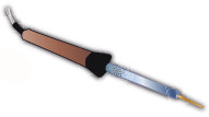
Ok, so we have your attention. These hints will help you to make this project successful. Read them carefully.- Make sure you have the right tools:

• A good quality soldering iron (25-40W) with a small tip.
• Wipe it often on a wet sponge or cloth, to keep it clean; then apply solder to the tip, to give it a wet look. This is called ‘thinning’ and will protect the tip and enables you to make good connections. When solder rolls off the tip, it needs cleaning.
• Thin raisin-core solder. Do not use any fl UX or grease.
• A diagonal cutter to trim excess wires. To avoid injury when cutting excess leads, hold the lead so they cannot fl y towards the eyes.
• Needle nose pliers, for bending leads, or to hold components in place.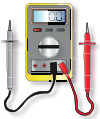
• Small blade and Phillips screwdrivers. A basic range is fine.
For some projects, a basic multi-meter is required or might be handy. - Assembly Hints :
• Make sure the skill level matches your experience, to avoid disappointments.
• Follow the instructions carefully. Read and understand the entire step before you perform each operation.
• Perform the assembly in the correct order as stated in this manual.
• Position all parts on the PCB (Printed Circuit Board) as shown on the drawings.
• Values on the circuit diagram are subject to changes, the values in this assembly guide are correct*.
• Use the check-boxes to mark your progress.
• Please read the included information on safety and customer service.
* Typographical inaccuracies excluded. Always look for possible last-minute manual updates, indicated as ‘NOTE’ on a separate leafl et. 1.3 - Soldering Hints :
1. Mount the component against the PCB surface and carefully solder the leads.
2. Make sure the solder joints are cone-shaped and shiny.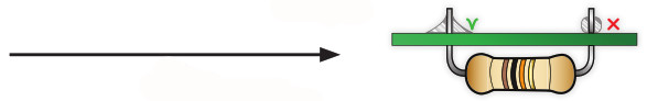
3. Trim excess leads as close as possible to the solder joint.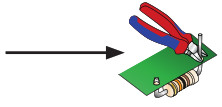
- Make sure you have the right tools:
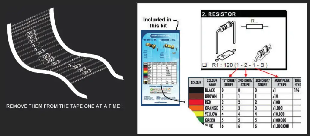
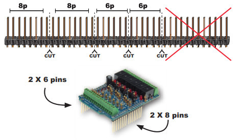
DO NOT BLINDLY FOLLOW THE ORDER OF THE COMPONENTS ON THE TAPE. ALWAYS CHECK THEIR VALUE ON THE PARTS LIST!
CONSTRUCTION
- Ceramic capacitor
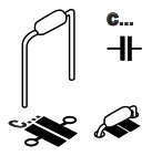 • C2: 100nF (104)
 - Diodes

Watch the polarity!
• D1: 1N4148
• D2: 1N4148
• D3 : 1N4148
• D4: 1N4148
• D5: 1N4148
• D6: 1N4148• D7: 1N4148
• D8: 1N4148
• D9: 1N4148
• D10: 1N4148
• D11: 1N4148
• D12: 1N4148 - Zenerdiodes
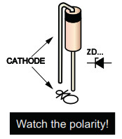
• ZD1 : 5V1
• ZD2 : 5V1
• ZD3 : 5V1• ZD4 : 5V1
• ZD5 : 5V1
• ZD6 : 5V1 - LED
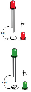
• LD1 : Red
• LD2 : Red
• LD3 : Red
• LD4 : Red
• LD5 : Red
• LD6 : RedWatch the polarity!
• LD7 : Green
• LD8 : Green
• LD9 : Green
• LD10 : Green
•LD11 : Green
• LD12 : Green - Transistors
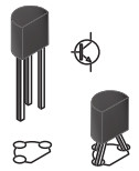
• T1: BC547B
• T2: BC547B
• T3: BC547B• T4: BC547B
• T5: BC547B
• T6: BC547B - Resistors
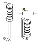
• R1 : 1K (1 – 0 – 2 – B)
• R2 : 1K (1 – 0 – 2 – B)
• R3 : 1K (1 – 0 – 2 – B)
• R4 : 1K (1 – 0 – 2 – B)
• R5 : 1K (1 – 0 – 2 – B)
• R6 : 1K (1 – 0 – 2 – B)
• R7: 4K7 (4 – 7 – 2 – B)
• R8 : 10K (1 – 0 – 3 – B)
• R9 : 4K7 (4 – 7 – 2 – B)
• R10 : 10K (1 – 0 – 3 – B)• R11 : 4K7 (4 – 7 – 2 – B)
• R12 : 10K (1 – 0 – 3 – B)
• R13 : 4K7 (4 – 7 – 2 – B)
• R14 : 10K (1 – 0 – 3 – B)
• R15: 4K7 (4 – 7 – 2 – B)
• R16 : 10K (1 – 0 – 3 – B)
• R17: 4K7 (4 – 7 – 2 – B)
• R18 : 10K (1 – 0 – 3 – B)
• R19 : 470 (4 – 7 – 1 – B)
• R20 : 470 (4 – 7 – 1 – B)• R21 : 470 (4 – 7 – 1 – B)
• R22 : 470 (4 – 7 – 1 – B)
• R23 : 470 (4 – 7 – 1 – B)
• R24 : 470 (4 – 7 – 1 – B)
• R25 : 4K7 (4 – 7 – 2 – B)
• R26: 4K7 (4 – 7 – 2 – B)
• R27 : 4K7 (4 – 7 – 2 – B)
• R28 : 4K7 (4 – 7 – 2 – B)
• R29 : 4K7 (4 – 7 – 2 – B)
•R30 : 4K7 (4 – 7 – 2 – B) - Terminal blocks
- Relays
- Electrolytic capacitors

• RY1
• RY2
• RY3• RY4
• RY5
• RY6Watch the polarity!
• C1: 100µF - Male header
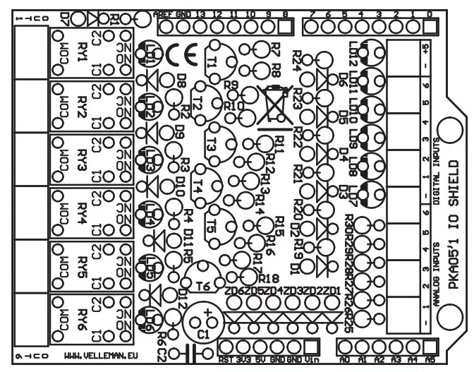
CONNECTION DIAGRAM
 DOWNLOAD SAMPLE CODE FROM KA05 PAGE ON WWW.VELLEMAN.BE
schematic diagram

PCB
![]() The new Velleman Projects catalogue is
The new Velleman Projects catalogue is
now available. Download your copy here:
www.vellemanprojects.eu

Modifi cations and typographical errors reserved – © Velleman nv. HKA05’IP (rev.4) Velleman NV, Legen Heirweg 33 – 9890 Gavere.
Documents / Resources
 | WHADDA KA05 Expansion Module [pdf] Instruction Manual KA05 Expansion Module, KA05, Expansion Module |


