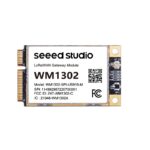
Ushine UP100 LoRaWAN Gateway Module User Manual
UP100 LoRaWAN Gateway Module users manual
Introduction
UP100 is a LoRaWAN Gateway Module with mini-PCIe form factor based on Semtech SX1303 and SX1261 for Listen Before Talk feature, which enables easy integration into an existing router or other network equipment with LPWAN Gateway capabilities. It can be used in any embedded platform offering a free mini-PCIe slot with USB/SPI connection. Furthermore, ZOE-M8Q GPS chip is integrated onboard.
This module is an complete and cost-efficient gateway solution offering up to 10 programmable parallel demodulation paths, 8 x 8 channel LoRa packet detectors, 8 x SF5-SF12 LoRa demodulators, and 8 x SF5-SF10 LoRa demodulators. It is capable of detecting an uninterrupted combination of pockets at 8 different spreading factors and 10 channels with continuous demodulation of up to 16 packets. This product is best for smart metering fixed networks and internet-of-Things (IoT) applications.
Features
- Designed based on mini-PCIe form factor
- Tx power up to 20.91dBm @SF12, BW 500KHz
- Supports global license-free frequency band (US915, AS923, AU915, KR920)
- Supports optional USB/SPI interfaces
- Listen Before Talk
- Fine Timestamp
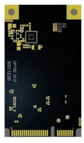
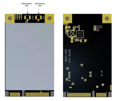
Board Overview
UP100 is a compact LoRaWAN Gateway Module, making it suitable for integration in systems where mass and size constraints are essential. It has been designed with the mini-PCIe form factor, so it can easily become a part of products that comply with the standard, where they allow for cards with a thickness of at least 5.2mm.
The board has two UFL interfaces for the LoRa and GNSS antennas and a standard 52 pin connector (mini-PCIe).
Block Diagram
The UP100 LoRaWAN gateway module is equipped with one SX1303 chip and two SX1250s. The first chip is utilized for the RF signal and the core of the device, while the latter provides the related LoRa modem and processing functionalities. Additional signal conditioning circuitry is implemented for PCI Express Mini Card compliance, and one UFL connectors are available for external antenna integration.

Figure 2: Block Diagram
Hardware
The hardware is categorized into several parts. It discusses the interfacing, pinouts, and its corresponding functions and diagrams. It also covers the parameters and standard values of the board.
Interfaces
- SPI Interface – SPI interface mainly provides for the HOST_SCK, HOST_MISO, HOST_MOSI, HOST_CSN pins of the system connector. The SPI interface gives access to the configuration register of SX1303 via a synchronous full-duplex protocol. Only the slave side is implemented.
- USB Interface – The USB interface mainly provides for the USB_D+, USB_D- pins of the system connector. The USB interface gives the access the configuration register of SX1303 via an MCU STM32L412. Only the slave side is implemented.
- UART and I2C interface – UP100 integrates a ZOE-M8Q GPS module which has UART and I2C interface. The PINs on the golden finger provide a UART connection and an I2C connection, which allows direct access to the GPS module. The PPS signal is not only connected to SX1303 internally but also connected to the golden finger which can be used by the host board.
- GPS_PPS – UP100 includes the PPS input for received packets time-stamped and Fine Timestamp.
- RESET – UP100 SPI card includes the RESET active-high input signal to reset the radio operations as specified by the SX1303 Specification. UP100 USB card’s RESET is controlled by MCU.
- Antenna RF Interface – The module have one RF interface over a standard UFL connector with a characteristic impedance of 50Ω. The RF port supports both Tx and Rx, providing the antenna interface.
Pinout Diagram

Figure 3: Pinout Diagram
Pinout Description
| Type | Description |
| IO | Bidirectional |
| DI | Digital input |
| DO | Digital output |
| OC | Open collector |
| OD | Open drain |
| PI | Power input |
| PO | Power output |
| NC | No connection |
| Pin No. | UP100 | Type | Description | Remarks |
| 1 | SX1261_BUSY | DO | No connection by default | Reserved for future applications |
| 2 | 3V3 | PI | 3.3V DC supply | |
| 3 | SX1261_DIO1 | IO | No connection by default | Reserved for future applications |
| 4 | GND | Ground | |||
| 5 | SX1261_DIO2 | IO | No connection by default | Reserved for future applications | |
| 6 | GPIO(6) | IO | No connection by default | Connect to the SX1302’s GPIO(6) | |
| 7 | SX1261_NSS | DI | No connection by default | Reserved for future applications | |
| 8 | NC | No connection | |||
| 9 | GND | Ground | |||
| 10 | NC | No connection | |||
| 11 | SX1261_NRESET | DI | No connection by default | Reserved for future applications | |
| 12 | NC | No connection | |||
| 13 | MCU_NRESET | DI | RESET signal for MCU of UP100-US915U | Active low | |
| 14 | NC | No connection | |||
| 15 | GND | Ground | |||
| 16 | NC | No connection | |||
| 17 | NC | No connection | |||
| 18 | GND | Ground | |||
| 19 | PPS | DO | Time pulse output | Leave open if not in use | |
| 20 | NC | No connection | |||
| 21 | GND | Ground | |||
| 22 | SX1303_RESET | DI | SX1303_RESET | Active high, ≥100ns for SX1302 reset | |
| 23 | RESET_GPS | DI | GSP module ZOE-M8Q reset input | Active low, leave open if not in use | |
| 24 | 3V3 | PI | 3.3V DC supply | ||
| 25 | STANDBY_GPS | DI | GPS module ZOE-M8Q external interrupt input | Active low, leave open if not in use | |
| 26 | GND | Ground | |||
| 27 | GND | Ground | |||
| 28 | GPIO(8) | Connect to the SX1303’s GPIO(8) | |||
| 29 | GND | Ground | |||
| 30 | I2C_CLK | IO | HOST CLK | Connect to GPS module ZOE-M8Q’s SCL internally, leave open if not in use | |
| 31 | UART_TX | DI | HOST UART_TX | Connect to GPS module ZOE-M8Q’s UART_RX internally, leave open if not in use | |
| 32 | I2C_DATA | IO | HOST DATA | Connect to GPS module ZOE-M8Q’s SDA internally, leave open if not in use | |
| 33 | UART_RX | DO | HOST UART_RX | Connect to GPS module |
| ZOE-M8Q’s UART_TX internally, leave open if not in use | |||||
| 34 | GND | Ground | |||
| 35 | GND | Ground | |||
| 36 | USB_DM | IO | USB differential data (-) | Require differential impedance of 90Ω | |
| 37 | GND | Ground | |||
| 38 | USB_DP | IO | USB differential data (+) | Require differential impedance of 90Ω | |
| 39 | 3V3 | PI | 3.3V DC supply | ||
| 40 | GND | Ground | |||
| 41 | 3V3 | PI | 3.3V DC supply | ||
| 42 | NC | No connection | |||
| 43 | GND | Ground | |||
| 44 | NC | No connection | |||
| 45 | HOST_SCK | IO | Host SPI SCK | ||
| 46 | NC | No connection | |||
| 47 | HOST_MISO | IO | Host SPI MISO | ||
| 48 | NC | No connection | |||
| 49 | HOST_MOSI | IO | Host SPI MOSI | ||
| 50 | GND | Ground | |||
| 51 | HOST_CSN | IO | Host SPI CSN | ||
| 52 | 3V3 | PI | 3.3V DC supply |
Operating Frequencies
The board supports the following LoRaWAN frequency channels, allowing easy configuration while building the firmware from the source code.
| Region | Frequency (MHz) |
| North America | US915 |
| Asia | AS923 |
| Australia | AU915 |
| Korea | KR920 |
RF Characteristics
The following table gives typically sensitivity level of the UP100 concentrator module.
| Signal bandwidth (KHz) | Spreading factor | Sensitivity (dBm) |
| 125 | 12 | -139 |
| 125 | 7 | -125 |
| 250 | 7 | -123 |
| 500 | 12 | -134 |
| 500 | 7 | -120 |
Electrical Requirements
Stressing the device above one or more of the ratings listed in the Absolute Maximum Rating section may cause permanent damage. These are stress ratings only. Operating the module at these or any conditions other than those specified in the Operating Conditions sections of the specification should be avoided. Exposure to Absolute Maximum Rating conditions for extended periods may affect device reliability.
The operating condition range defines those limits within which the functionality of the device is guaranteed. Where application information is given, it is advisory only and does not form part of the specification.
Absolute Maximum Rating
The limiting values given below are following the Absolute Maximum Rating System (IEC 134).
| Symbol | Description | Condition | Min | Max |
| 3V3 | Module supply voltage | Input DC voltage at 3V3 pins | -0.3V | 3.6V |
| USB | USB D+/D- pins | Input DC voltage at USB interface pins | 3.6V | |
| RESET | UP100 reset pin | Input DC voltage at RESET input pin | -0.3V | 3.6V |
| SPI | SPI interface | Input DC voltage at SPI interface pin | -0.3V | 3.6V | |
| GPS_PPS | GPS PPS input | Input DC voltage at GPS_PPS input pin | -0.3V | 3.6V | |
| Pho_ANT | Antenna ruggedness | Output RF load mismatch ruggedness at ANT1 | 10:1 VSWR | ||
| Tstg | Storage temperature | -40 °C | 85 °C |
WARNING:
The product is not protected against overvoltage or reversed voltages. If necessary, voltage spikes exceeding the power supply voltage specification, given in table above, must be limited to values within the specified boundaries by using appropriate protection devices
Maximum ESD
| Parameter | Min | Typical | Max | Remarks |
| ESD_HBM | 1000V | Charged Device Model JESD22-C101 CLASS III | ||
| ESD_CDM | 1000V | Charged Device Model JESD22-C101 CLASS III |
NOTE:
Although this module is designed to be as robust as possible, electrostatic discharge (ESD) can damage this module. This module must be protected at all times from ESD when handling or transporting. Static charges may easily produce potentials of several kilovolts on the human body or equipment, which can discharge without detection. Industry-standard ESD handling precautions should be used at all times.
Power Consumption
| Mode | Condition | Min | Typical | Max |
| Active mode (TX) | The power of the TX channel is 20 dBm and 3.3V supply. | 511mA | 512mA | 513mA |
| Active mode (RX) | TX disabled and RX enabled | 70mA | 81.6mA | 101mA |
Power Supply Range
Input voltage at 3V3 must be above the normal operating range minimum limit to switch on the module.
| Symbol | Parameter | Min | Typical | Max |
| 3V3 | Module supply operating input voltage | 3V | 3.3V | 3.6V |
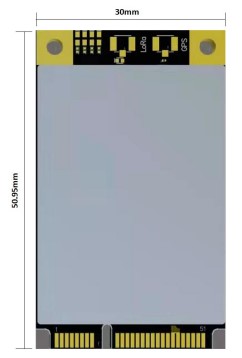
Mechanical Characteristics
The board weighs 8.5 grams, it is 30 mm wide and 50.95 mm tall. The dimensions of the module fall completely within the PCI Express Mini Card Electromechanical Specification, except for the card’s thickness (maximum 5.2 mm at its thickest).
Operating Conditions
| Parameter | Min | Typical | Max | Remarks |
| Normal operating Temperature | -40 °C | +25 °C | +85 °C | Normal operating temperature range (fully functional and meet 3GPP specifications) |
NOTE:
Unless otherwise indicated, all operating condition specifications are at an ambient temperature of 25°C. Operation beyond the operating conditions is not recommended and extended exposure beyond them may affect device reliability.
Schematic Diagram
UP100 gateway module refers to Semtech’s reference design for SX1303. The SPI interface can be used on the mini-PCIe connector. The next figure shows the minimum application schematic of the UP100. You should use at least 3.3V/1A DC power, connect the SPI interface to the main processor.

Figure 5: Schematic Diagram
Federal Communication Commission Interference Statement
This device complies with Part 15 of the FCC Rules. Operation is subject to the following two conditions: (1) This device may not cause harmful interference, and (2) this device must accept any interference received, including interference that may cause undesired operation.
This equipment has been tested and found to comply with the limits for a Class B digital device, pursuant to Part 15 of the FCC Rules. These limits are designed to provide reasonable protection against harmful interference in a residential installation. This equipment generates, uses and can radiate radio frequency energy and, if not installed and used in accordance with the instructions, may cause harmful interference to radio communications. However, there is no guarantee that interference will not occur in a particular installation. If this equipment does cause harmful interference to radio or television reception, which can be determined by turning the equipment off and on, the user is encouraged to try to correct the interference by one of the following measures:
- Reorient or relocate the receiving
- Increase the separation between the equipment and
- Connect the equipment into an outlet on a circuit different from that to which the receiver is
- Consult the dealer or an experienced radio/TV technician for
FCC Caution: Any changes or modifications not expressly approved by the party responsible for compliance could void the user’s authority to operate this equipment.
This transmitter must not be co-located or operating in conjunction with any other antenna or transmitter.
Radiation Exposure Statement:
This equipment complies with FCC radiation exposure limits set forth for an uncontrolled environment. This equipment should be installed and operated with minimum distance 20cm between the radiator & your body.
This device is intended only for OEM integrators under the following conditions:
- The antenna must be installed such that 20 cm is maintained between the antenna and users, and
- The transmitter module may not be co-located with any other transmitter or antenna.
- Module approval valid only when the module is installed in the tested host or compatible series of host
As long as 3 conditions above are met, further transmitter test will not be required. However, the OEM integrator is still responsible for testing their end-product for any additional compliance requirements required with this module installed
IMPORTANT NOTE: In the event that these conditions can not be met (for example certain laptop configurations or co-location with another transmitter), then the FCC authorization is no longer considered valid and the FCC ID can not be used on the final product. In these circumstances, the OEM integrator will be responsible for re-evaluating the end product (including the transmitter) and obtaining a separate FCC authorization.
End Product Labeling
This transmitter module is authorized only for use in device where the antenna may be installed such that 20 cm may be maintained between the antenna and users. The final end product must be labeled in a visible area with the following: “Contains FCC ID:

Manual Information To the End User
2A5CK-UP100”. The grantee’s FCC ID can be used only when all FCC compliance requirements are met.
The OEM integrator has to be aware not to provide information to the end user regarding how to install or remove this RF module in the user’s manual of the end product which integrates this module.
The end user manual shall include all required regulatory information/warning as show in this manual.
Read More About This Manual & Download PDF:
Documents / Resources
 | Ushine UP100 LoRaWAN Gateway Module [pdf] User Manual UP100, 2A5CK-UP100, 2A5CKUP100, UP100 LoRaWAN Gateway Module, UP100, LoRaWAN Gateway Module |