![]()
WL2862E
High Input Voltage, Low Quiescent Current LDO
Descriptions
The WL2862E series is a high accuracy, high input voltage low quiescent current, high speed, and low dropout Linear regulator with high ripple rejection.
The WL2862E offers over-current limit and over temperature protection to ensure the device working in well conditions.
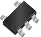
The WL2862E regulators are available in standard SOT-23-5L packages. Standard products are Pb-free and Halogen-free.
| SOT-23-5L |
Features
- Supply Voltage : 4.5V~36V
- Output Range : 3V~12V
- Output Accuracy : <+/-2%
- Output Current : 150mA@(VIN-VOUT=2V)(Typ.)
- PSRR : 65dB @ 0.1KHz
- Dropout Voltage : 1000mV @ IOUT=150mA
- Quiescent Current : 4.5μA@VIN=12V(Typ.)
- Recommend Capacitor : 10uF
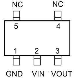
Pin Configuration (Top View)
Order Information
For detail order information, please see page 10.
Applications
- Battery-Powered Equipment
- Communication Equipment
- Audio/Video Equipment
- Smoke Detector
Typical Application

(Locate Cin and Cout as close to the Vin pin and Vout pin as possible.)
Pin Description
| PIN | Symbol | Description |
| 1 | GND | Ground |
| 2 | VIN | Voltage Input |
| 3 | VOUT | Voltage Output |
| 4 | NC | Not Connect |
| 5 | NC | Not Connect |
Block Diagram

Absolute Maximum Ratings
| Parameter | Value | Unit |
| Power Dissipation | 500 | mW |
| VIN Range | -0.3~44 | V |
| VOUT Range | -0.3~15 | V |
| Lead Temperature Range | 260 | ℃ |
| Storage Temperature Range | -55 ~ 150 | ℃ |
| Operating Junction Temperature Range | 150 | ℃ |
| ESD MM | 600 | V |
| ESD HBM | 8K | V |
Recommend Operating Ratings
| Parameter | Value | Unit |
| Operating Supply voltage | 4.5~36 | V |
| Operating Temperature Range | -40~85 | ℃ |
| Thermal Resistance (On PCB) , RθJA | 250 | ℃/W |
Electronics Characteristics
(Ta=25℃, VIN=12V,VOUT=5.0V, CIN=COUT=10uF, unless otherwise noted)
| Symbol | Parameter | Test Condition | WL2862E SPEC | Unit | |||
| Min. | Typ. | Max. | |||||
| VIN | Input Range | lour=lOmA | 4.5 | 36 | V | ||
| VOUT | Output Range | louT=10mA | VouT*0.98 | VOuT | VOUT*1.02 | V | |
| ΔVOUT | Output Voltage | VIN=12V,louT=lOmA | 2.940 | 3.0 | 3.060 | ||
| 3.234 | 3.3 | 3.366 | V | ||||
| 4.9 | 5.0 | 5.1 | V | ||||
| VIN=18V,IouT=10mA | 9.8 | 10.0 | 10.2 | V | |||
| IOUT_PK | Maximum Output Current | VIN= VouT.2V, RL=10 | 150 | mA | |||
| IQ1 | Quiescent Current For Vour=5V | VIN=12V, No load | 4.5 | μA | |||
| IQ2 | Quiescent Current For VouT=10V | V1N=18V, No load | 5.5 | μA | |||
| VDROP | Dropout Voltage | louT=1mA | 6.5 | mV | |||
| louT=150mA | 1000 | ||||||
| △VLine | Line Regulation | VIN=7-24V,Vour=5V louT=l mA | 0.02 | %/V | |||
| VIN=7–36V,VouT=5V louT=1mA | 0.1 | ||||||
| △VLoad | Load Regulation | VIN=12V, [OUT= 1–100mA | 0.6 | % | |||
| eNO | Output Noise | louT=10mA | 300 | μV | |||
| PSRR | Ripple Rejection | VIN=10.0V Vpp=0.5V louT=1mA | f=100Hz | 65 | dB | ||
| f=1KHz | 55 | ||||||
| f=10KHz | 40 | ||||||
| Tso | Thermal Protection | VIN =12V, louT=1mA | 150 | ℃ | |||
| ΔVo/ΔT | Temperature Coefficient | VIN=12V, louT=1mA | 100 | ppm | |||
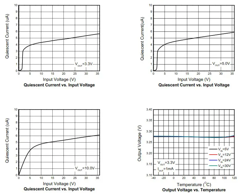
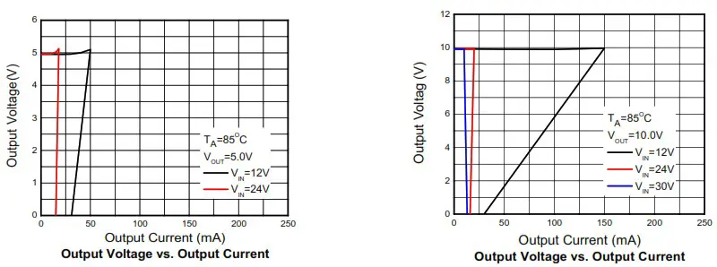
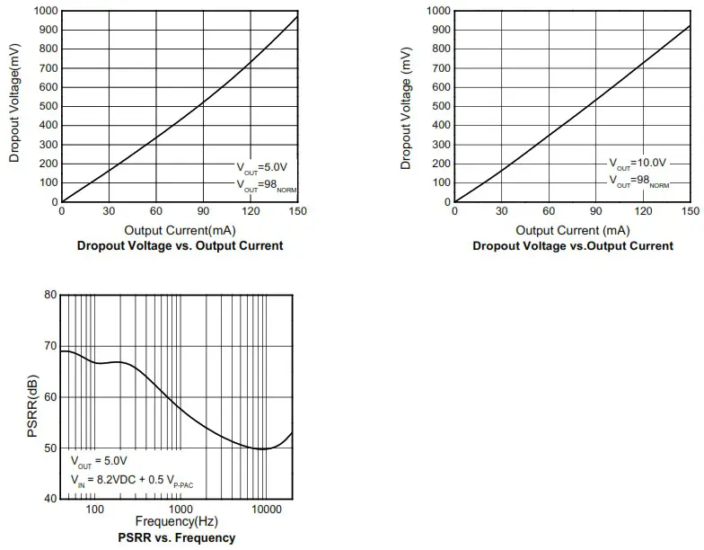
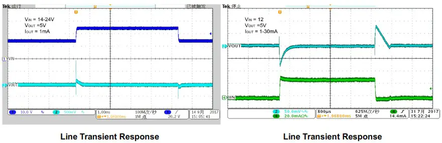
Typical characteristics
(Ta=25℃,CIN=COUT=10uF, unless otherwise noted)

ORDER INFORMATION
| Ordering No. | Vout (V) | Package | Operating Temperature | Marking | Shipping |
| WL2862E30-5/TR | 3.0 | SOT-23-5L | -40–+85°C | 2862 EMYW | Tape and Reel, 3000 |
| WL2862E33-5/TR | 3. | SOT-23-5L | -40–+85°C | 2862 ENYW | Tape and Reel, 3000 |
| WL2862E50-5/TR | 5.0 | SOT-23-5L | -40-+85°C | 2862 ETYW | Tape and Reel, 3000 |
| WL2862EA0-5/TR | 10.0 | SOT-23-5L | -40-+85°C | 2862 EZYW | Tape and Reel, 3000 |
PACKAGE OUTLINE DIMENSIONS
SOT-23-5L
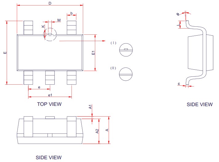
| Symbol | Dimensions in Millimeters | ||
| Min. | Typ. | Max. | |
| A | – | – | 1.45 |
| Al | 0.00 | – | 0.15 |
| A2 | 0.90 | 1.10 | 1.30 |
| b | 0.30 | 0.40 | 0.50 |
| c | 0.10 | – | 0.21 |
| D | 2.72 | 2.92 | 3.12 |
| E | 2.60 | 2.80 | 3.00 |
| El | 1.40 | 1.60 | 1.80 |
| e | 0.95 BSC | ||
| el | 1.90 BSC | ||
| L | 0.30 | 0.45 | 0.60 |
| M | 0.10 | 0.15 | 0.25 |
| K | 0.00 | – | 0.25 |
| 0 | 0° | – | 8° |
TAPE AND REEL INFORMATION
Reel Dimensions

Tape Dimensions
Quadrant Assignments For PIN1 Orientation In Tape

| RD | Reel Dimension | |
| W | Overall width of the carrier tape | |
| P1 | Pitch between successive cavity centers | |
| Pin1 | Pin1 Quadrant |
4275 Burton Drive Santa Clara, CA 95054 USA
Tel: + 1 408 567 3000
Fax: + 1 408 567 3001
www.ovt.com
OMNIVISION reserves the right to make changes to their products or to discontinue any product or service without further notice. OMNIVISION and the OMNIVISION logo are trademarks or registered trademarks of OmniVision Technologies, Inc. All other trademarks are the property of their respective owners.
![]()
Documents / Resources
 | OmniVision WL2862E Cube Chip Image Sensor ASIC Camera [pdf] Instruction Manual WL2862E Cube Chip Image Sensor ASIC Camera, WL2862E, Cube Chip Image Sensor ASIC Camera, Chip Image Sensor ASIC Camera, Sensor ASIC Camera, ASIC Camera, Camera |