intel Native Loopback Accelerator Functional Unit (AFU)

About this Document
Conventions
Table 1. Document Conventions
| Convention | Description |
| # | Precedes a command that indicates the command is to be entered as root. |
| $ | Indicates a command is to be entered as a user. |
| This font | Filenames, commands, and keywords are printed in this font. Long command lines are printed in this font. Although long command lines may wrap to the next line, the return is not part of the command; do not press enter. |
| <variable_name> | Indicates the placeholder text that appears between the angle brackets must be replaced with an appropriate value. Do not enter the angle brackets. |
Acronyms
Table 2. Acronyms
| Acronyms | Expansion | Description |
| AF | Accelerator Function | Compiled Hardware Accelerator image implemented in FPGA logic that accelerates an application. |
| AFU | Accelerator Functional Unit | Hardware Accelerator implemented in FPGA logic which offloads a computational operation for an application from the CPU to improve performance. |
| API | Application Programming Interface | A set of subroutine definitions, protocols, and tools for building software applications. |
| ASE | AFU Simulation Environment | Co-simulation environment that allows you to use the same host application and AF in a simulation environment. ASE is part of the Intel® Acceleration Stack for FPGAs. |
| CCI-P | Core Cache Interface | CCI-P is the standard interface AFUs use to communicate with the host. |
| CL | Cache Line | 64-byte cache line |
| DFH | Device Feature Header | Creates a linked list of feature headers to provide an extensible way of adding features. |
| FIM | FPGA Interface Manager | The FPGA hardware containing the FPGA Interface Unit (FIU) and external interfaces for memory, networking, etc. The Accelerator Function (AF) interfaces with the FIM at run time. |
| FIU | FPGA Interface Unit | FIU is a platform interface layer that acts as a bridge between platform interfaces like PCIe*, UPI and AFU-side interfaces such as CCI-P. |
| continued… | ||
Intel Corporation. All rights reserved. Intel, the Intel logo, and other Intel marks are trademarks of Intel Corporation or its subsidiaries. Intel warrants performance of its FPGA and semiconductor products to current specifications in accordance with Intel’s standard warranty, but reserves the right to make changes to any products and services at any time without notice. Intel assumes no responsibility or liability arising out of the application or use of any information, product, or service described herein except as expressly agreed to in writing by Intel. Intel customers are advised to obtain the latest version of device specifications before relying on any published information and before placing orders for products or services. *Other names and brands may be claimed as the property of others.
| Acronyms | Expansion | Description |
| MPF | Memory Properties Factory | The MPF is a Basic Building Block (BBB) that AFUs can use to provide CCI-P traffic shaping operations for transactions with the FIU. |
| Msg | Message | Message – a control notification |
| NLB | Native Loopback | The NLB performs reads and writes to the CCI-P link to test connectivity and throughput. |
| RdLine_I | Read Line Invalid | Memory Read Request, with FPGA cache hint set to invalid. The line is not cached in the FPGA, but may cause FPGA cache pollution. Note: The cache tag tracks the request status for all outstanding requests on Intel Ultra Path Interconnect (Intel UPI). Therefore, even though RdLine_I is marked invalid upon completion, it consumes the cache tag temporarily to track the request status over UPI. This action may result in the eviction of a cache line, resulting in cache pollution. The advantage of using RdLine_I is that it is not tracked by CPU directory; thus it prevents snooping from CPU. |
| RdLine-S | Read Line Shared | Memory read request with FPGA cache hint set to shared. An attempt is made to keep it in the FPGA cache in a shared state. |
| WrLine_I | Write Line Invalid | Memory Write Request, with FPGA cache hint set to Invalid. The FIU writes the data with no intention of keeping the data in FPGA cache. |
| WrLine_M | Write Line Modified | Memory Write Request, with the FPGA cache hint set to Modified. The FIU writes the data and leaves it in the FPGA cache in a modified state. |
Acceleration Glossary
Table 3. Acceleration Stack for Intel Xeon® CPU with FPGAs Glossary
| Term | Abbreviation | Description |
| Intel Acceleration Stack for Intel Xeon® CPU with FPGAs | Acceleration Stack | A collection of software, firmware, and tools that provides performance- optimized connectivity between an Intel FPGA and an Intel Xeon processor. |
| Intel FPGA Programmable Acceleration Card (Intel FPGA PAC) | Intel FPGA PAC | PCIe FPGA accelerator card. Contains an FPGA Interface Manager (FIM) that pairs with an Intel Xeon processor over the PCIe bus. |
The Native Loopback Accelerator Functional Unit (AFU)
Native Loopback (NLB) AFU Overview
- The NLB sample AFUs comprise a set of Verilog and System Verilog files to test memory reads and writes, bandwidth, and latency.
- This package includes three AFUs that you can build from the same RTL source. Your configuration of the RTL source code creates these AFUs.
The NLB Sample Accelerator Function (AF)
The $OPAE_PLATFORM_ROOT/hw/samples directory stores source code for the following NLB sample AFUs:
- nlb_mode_0
- nlb_mode_0_stp
- nlb_mode_3
Note: The $DCP_LOC/hw/samples directory stores the NLB sample AFUs source code for the 1.0 release package.
To understand the NLB sample AFU source code structure and how to build it, refer to one of the following Quick Start Guides (depending on which Intel FPGA PAC you are using):
- If you are using Intel PAC with Intel Arria® 10 GX FPGA, refer to the IntelProgrammable Acceleration Card with Intel Arria 10 GX FPGA.
- If you are using Intel FPGA PAC D5005, refer to the Intel Acceleration Stack Quick Start Guide for Intel FPGA Programmable Acceleration Card D5005.
The release package provides the following three sample AFs:
- NLB mode 0 AF: requires hello_fpga or fpgadiag utility to perform the lpbk1 test.
- NLB mode 3 AF: requires fpgadiag utility to perform the trupt, read, and write tests.
- NLB mode 0 stp AF: requires hello_fpga or fpgadiag utility to perform the lpbak1 test.
Note: The nlb_mode_0_stp is the same AFU as nlb_mode_0 but with Signal Tap debug feature enabled.
The fpgadiag and hello_fpga utilities help the appropriate AF to diagnose, test and report on the FPGA hardware.
Intel Corporation. All rights reserved. Intel, the Intel logo, and other Intel marks are trademarks of Intel Corporation or its subsidiaries. Intel warrants performance of its FPGA and semiconductor products to current specifications in accordance with Intel’s standard warranty, but reserves the right to make changes to any products and services at any time without notice. Intel assumes no responsibility or liability arising out of the application or use of any information, product, or service described herein except as expressly agreed to in writing by Intel. Intel customers are advised to obtain the latest version of device specifications before relying on any published information and before placing orders for products or services. *Other names and brands may be claimed as the property of others.
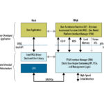
Figure 1. Native Loopback (nlb_lpbk.sv) Top Level Wrapper

Table 4. NLB Files
| File Name | Description |
| nlb_lpbk.sv | Top-level wrapper for NLB that instantiates the requestor and arbiter. |
| arbiter.sv | Instantiates the test AF. |
| requestor.sv | Accepts requests from the arbiter and formats the requests according to the CCI-P specification. Also implements flow control. |
| nlb_csr.sv | Implements a 64-bit read/write Control and Status (CSR) registers. The registers support both 32- and 64-bit reads and writes. |
| nlb_gram_sdp.sv | Implements a generic dual-port RAM with one write port and one read port. |
NLB is a reference implementation of an AFU compatible with the Intel Acceleration Stack for Intel Xeon CPU with FPGAs Core Cache Interface (CCI-P) Reference Manual. NLB’s primary function is to validate host connectivity using different memory access patterns. NLB also measures bandwidth and read/write latency. The bandwidth test has the following options:
- 100% read
- 100% write
- 50% read and 50% writes
Related Information
- Intel Acceleration Stack Quick Start Guide for Intel Programmable Acceleration Card with Arria 10 GX FPGA
- Acceleration Stack for Intel Xeon CPU with FPGAs Core Cache Interface (CCI-P) Reference Manual
- Intel Acceleration Stack Quick Start Guide for Intel FPGA Programmable Acceleration Card D5005
Native Loopback Control and Status Register Descriptions
Table 5. CSR Names, Addresses and Descriptions
| Byte Address (OPAE) | Word Address (CCI-P) | Access | Name | Width | Description |
| 0x0000 | 0x0000 | RO | DFH | 64 | AF Device Feature Header. |
| 0x0008 | 0x0002 | RO | AFU_ID_L | 64 | AF ID low. |
| 0x0010 | 0x0004 | RO | AFU_ID_H | 64 | AF ID high. |
| 0x0018 | 0x0006 | Rsvd | CSR_DFH_RSVD0 | 64 | Mandatory Reserved 0. |
| 0x0020 | 0x0008 | RO | CSR_DFH_RSVD1 | 64 | Mandatory Reserved 1. |
| 0x0100 | 0x0040 | RW | CSR_SCRATCHPAD0 | 64 | Scratchpad register 0. |
| 0x0108 | 0x0042 | RW | CSR_SCRATCHPAD1 | 64 | Scratchpad register 2. |
| 0x0110 | 0x0044 | RW | CSR_AFU_DSM_BASE L | 32 | Lower 32-bits of AF DSM base address. The lower 6 bits are 4×00 because the address is aligned to the 64-byte cache line size. |
| 0x0114 | 0x0045 | RW | CSR_AFU_DSM_BASE H | 32 | Upper 32-bits of AF DSM base address. |
| 0x0120 | 0x0048 | RW | CSR_SRC_ADDR | 64 | Start physical address for source buffer. All read requests target this region. |
| 0x0128 | 0x004A | RW | CSR_DST_ADDR | 64 | Start physical address for destination buffer. All write requests target this region |
| 0x0130 | 0x004C | RW | CSR_NUM_LINES | 32 | Number of cache lines. |
| 0x0138 | 0x004E | RW | CSR_CTL | 32 | Controls test flow, start, stop, force completion. |
| 0x0140 | 0x0050 | RW | CSR_CFG | 32 | Configures test parameters. |
| 0x0148 | 0x0052 | RW | CSR_INACT_THRESH | 32 | Inactivity threshold limit. |
| 0x0150 | 0x0054 | RW | CSR_INTERRUPT0 | 32 | SW allocates Interrupt APIC ID and Vector to device. |
| DSM Offset Map | |||||
| 0x0040 | 0x0010 | RO | DSM_STATUS | 32 | Test status and error register. |
Table 6. CSR Bit Fields with Examples
This table lists the CSR bit fields that depend on the value of the CSR_NUM_LINES, <N>. In the example below <N> = 14.
| Name | Bit Field | Access | Description |
| CSR_SRC_ADDR | [63:<N>] | RW | 2^(N+6)MB aligned address points to the start of the read buffer. |
| [<N>-1:0] | RW | 0x0. | |
| CSR_DST_ADDR | [63:<N>] | RW | 2^(N+6)MB aligned address points to the start of the write buffer. |
| [<N>-1:0] | RW | 0x0. | |
| CSR_NUM_LINES | [31:<N>] | RW | 0x0. |
| continued… | |||
| Name | Bit Field | Access | Description |
| [<N>-1:0] | RW | Number of cache lines to read or write. This threshold may be different for each test AF. Note: Ensure that source and destination buffers are large enough to accommodate the <N> cache lines. CSR_NUM_LINES should be less than or equal to <N>. | |
| For the following values, assume <N>=14. Then, CSR_SRC_ADDR and CSR_DST_ADDR accept 2^20 (0x100000). | |||
| CSR_SRC_ADDR | [31:14] | RW | 1MB aligned address. |
| [13:0] | RW | 0x0. | |
| CSR_DST_ADDR | [31:14] | RW | 1MB aligned address. |
| [13:0] | RW | 0x0. | |
| CSR_NUM_LINES | [31:14] | RW | 0x0. |
| [13:0] | RW | Number of cache lines to read or write. This threshold may be different for each test AF. Note: Ensure that source and destination buffers are large enough to accommodate the <N> cache lines. | |
Table 7. Additional CSR Bit Fields
| Name | Bit Field | Access | Description |
| CSR_CTL | [31:3] | RW | Reserved. |
| [2] | RW | Force test completion. Writes test completion flag and other performance counters to csr_stat. After forcing test completion, the hardware state is identical to a non-forced test completion. | |
| [1] | RW | Starts test execution. | |
| [0] | RW | Active low test reset. When low, all configuration parameters change to their default values. | |
| CSR_CFG | [29] | RW | cr_interrupt_testmode tests interrupts. Generates an interrupt at the end of each test. |
| [28] | RW | cr_interrupt_on_error sends an interrupt when upon error | |
| detection. | |||
| [27:20] | RW | cr_test_cfg configures the behavior of each test mode. | |
| [13:12] | RW | cr_chsel selects the virtual channel. | |
| [10:9] | RW | cr_rdsel configures the read request type. The encodings have the | |
| following valid values: | |||
| • 1’b00: RdLine_S | |||
| • 2’b01: RdLine_I | |||
| • 2’b11: Mixed mode | |||
| [8] | RW | cr_delay_en enables random delay insertion between requests. | |
| [6:5] | RW | Configures test mode,cr_multiCL-len. Valid values are 0,1,and 3. | |
| [4:2] | RW | cr_mode, configures test mode. The following values are valid: | |
| • 3’b000: LPBK1 | |||
| • 3’b001: Read | |||
| • 3’b010: Write | |||
| • 3’b011: TRPUT | |||
| continued… | |||
| Name | Bit Field | Access | Description |
| For more information about the test mode, refer to the Test Modes topic below. | |||
| [1] | RW | c_cont selects test rollover or test termination. • When 1’b0, the test terminates. Updates the status CSR when CSR_NUM_LINES count is reached. • When 1’b1, the test rolls over to the start address after it reaches the CSR_NUM_LINES count. In rollover mode, the test terminates only upon error. | |
| [0] | RW | cr_wrthru_en switches between WrLine_I and Wrline_M request types. • 1’b0: WrLine_M • 1’b1: WrLine_I | |
| CSR_INACT_THRESHOLD | [31:0] | RW | Inactivity threshold limit. Detects the duration of stalls during a test run. Counts the number of consecutive idle cycles. If the inactivity count > CSR_INACT_THRESHOLD, no requests are sent, no responses are received, and the inact_timeout signal is set. Writing 1 to CSR_CTL[1] activates this counter. |
| CSR_INTERRUPT0 | [23:16] | RW | The Interrupt Vector Number for the device. |
| [15:0] | RW | apic_id is the APIC OD for the device. | |
| DSM_STATUS | [511:256] | RO | Error dump form Test Mode. |
| [255:224] | RO | End Overhead. | |
| [223:192] | RO | Start Overhead. | |
| [191:160] | RO | Number of Writes. | |
| [159:128] | RO | Number of Reads. | |
| [127:64] | RO | Number of Clocks. | |
| [63:32] | RO | Test error register. | |
| [31:16] | RO | Compare and exchange success counter. | |
| [15:1] | RO | Unique ID for each DSM status write. | |
| [0] | RO | Test completion flag. |
Test Modes
CSR_CFG[4:2] configures the test mode. The following four tests are available:
- LPBK1: This is a memory copy test. The AF copies CSR_NUM_LINES from the source buffer to the destination buffer. Upon test completion, the software compares the source and destination buffers.
- Read: This test stresses the read path and measures read bandwidth or latency. The AF reads CSR_NUM_LINES starting from the CSR_SRC_ADDR. This is only a bandwidth or latency test. It does not verify the data read.
- Write: This test stresses the write path and measures write bandwidth or latency. The AF reads CSR_NUM_LINES starting from the CSR_SRC_ADDR. This is only a bandwidth or latency test. It does not verify the data written.
- TRPUT: This test combines the reads and writes. It reads CSR_NUM_LINES starting from CSR_SRC_ADDR location and writes CSR_NUM_LINES to CSR_SRC_ADDR. It also measures read and write bandwidth. This test does not check the data. The reads and writes have no dependencies
The following table shows the CSR_CFG encodings for the four tests. This table sets and CSR_NUM_LINES, <N>=14. You can change the number of cache lines by updating the CSR_NUM_LINES register.
Table 8. Test Modes
FPGA Diagnostics: fpgadiag
The fpgadiag utility includes several tests to diagnose, test, and report on the FPGA hardware. Use the fpgadiag utility to run all the test modes. For more information about using the fpgadiag utility, refer to the fpgadiag section in the Open Programmable Acceleration Engine (OPAE) Tools Guide.
NLB Mode0 Hello_FPGA Test Flow
- Software initializes Device Status Memory (DSM) to zero.
- Software writes the DSM BASE address to the AFU. CSR Write(DSM_BASE_H), CSRWrite(DSM_BASE_L)
- Software prepares source and destination memory buffer. This preparation is test specific.
- Software writes CSR_CTL[2:0]= 0x1. This write brings the test out of reset and into configuration mode. Configuration can proceed only when CSR_CTL[0]=1 & CSR_CTL[1]=1.
- Software configures the test parameters, such as src, destaddress, csr_cfg, num lines, and so on.
- Software CSR writes CSR_CTL[2:0]= 0x3. The AF begins test execution.
- Test completion:
- Hardware completes when the test completes or detects an error. Upon completion, the hardware AF updates DSM_STATUS. Software polls DSM_STATUS[31:0]==1 to detect test completion.
- Software can force test completion by writing CSR writes CSR_CTL[2:0]=0x7. Hardware AF updates DSM_STATUS.
Document Revision History for the Native Loopback Accelerator Functional Unit (AFU) User Guide
| Document Version | Intel Acceleration Stack Version | Changes |
| 2019.08.05 | 2.0 (supported with Intel Quartus Prime Pro Edition 18.1.2) and 1.2 (supported with Intel Quartus Prime Pro Edition 17.1.1) | Added support for the Intel FPGA PAC D5005 platform in the current release. |
| 2018.12.04 | 1.2 (supported with Intel Quartus® Prime Pro Edition 17.1.1) | Maintenance release. |
| 2018.08.06 | 1.1 (supported with Intel Quartus Prime Pro Edition 17.1.1) and 1.0 (supported with Intel Quartus Prime Pro Edition 17.0.0) | Updated the location of the source code for the NLB sample AFU in The NLB Sample Accelerator Function (AF) section. |
| 2018.04.11 | 1.0 (supported with Intel Quartus Prime Pro Edition 17.0.0) | Initial release. |
Intel Corporation. All rights reserved. Intel, the Intel logo, and other Intel marks are trademarks of Intel Corporation or its subsidiaries. Intel warrants performance of its FPGA and semiconductor products to current specifications in accordance with Intel’s standard warranty, but reserves the right to make changes to any products and services at any time without notice. Intel assumes no responsibility or liability arising out of the application or use of any information, product, or service described herein except as expressly agreed to in writing by Intel. Intel customers are advised to obtain the latest version of device specifications before relying on any published information and before placing orders for products or services. *Other names and brands may be claimed as the property of others.
Documents / Resources
 | intel Native Loopback Accelerator Functional Unit (AFU) [pdf] User Guide Native Loopback Accelerator Functional Unit AFU, Native Loopback, Accelerator Functional Unit AFU, Functional Unit AFU |