ANALOG DEVICES DC3195A-B Evaluation Board

General Description
The DC3195A-B evaluation board features the LTM®4652 μModule® (micromodule) regulator, which is configured as a quad polyphase single –5V output capable of bidirectional ±128A load current. The input voltage range is 4.5V to 13V. The maximum VIN + |VOUT| should not exceed 18V for this inverting output evaluation board. Derating is necessary for certain VIN, VOUT, frequency, and thermal conditions.
The DC3195A-B evaluation board can be configured to source or sink the output load current. Figure 2 and Figure 3 show the hardware test setup diagrams for both conditions, respectively. The evaluation board is optimized using a default frequency of 780kHz under the 9VIN and –5VOUT operating conditions. The LTM4652 current mode architecture is peak current mode control. The evaluation board operates in continuous current mode (CCM) by default, but it can be placed in pulse-skipping mode (PSM) to optimize efficiency at light loads. The LTM4652 is available in a thermally enhanced 144-pin (16mm × 16mm × 4.92mm) BGA package. Temperature sensing options are included through the onboard circuit.
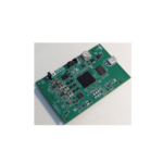
Evaluation Board Photo

The LTM4652 features an exposed metal top which is electrically unconnected for heatsinking capability.The inverting configuration feature of the LTM4652 has a different maximum current limit compared to the noninverting configuration feature. (Refer to DN1021 for more information). The LTM4652 data sheet gives a complete description of the device. The data sheet and this user guide must be read before using or making any hardware changes to the DC3195A-B evaluation board.
Features and Benefits
- ±128A Sourcing and Sinking Current
- Parallel for High-Power Applications
DC3195A-B Evaluation Board Files
| FILE | DESCRIPTION |
| DC3195A-B | Evaluation board files. |
Performance Summary
Specifications are at TA = 25°C
| PARAMETER | SYMBOL | CONDITIONS | MIN | TYP | MAX | UNIT |
| Input voltage range | VIN | 4.5 | 9 | 13 | V | |
| Output voltage | VOUT | RFB = 8.06kΩ | –5 | V | ||
| Switching frequency | fSW | fSET connected to INTVCC | 780 | kHz | ||
| Maximum output current | ABOUT | VIN = 9V, VOUT = –5V, fSW = 780kHz | ±128 | A | ||
| Efficiency | ||||||
| Sourcing current | η | VIN = 12V, IOUT = 128A, fSW = 780kHz | 89.8 | % | ||
| Sinking current | η | VIN = 12V, IOUT = –128A, fSW = 780kHz | 90 | % | ||
Quick Start
Required Equipment
- Two power supplies
- Two electronic loads
- Two digital multimeters (DMMs)
- One high-current diode (sinking condition)
Quick Start Procedure
The DC3195A-B evaluation board is an easy way to evaluate the performance of the LTM4652 in a multiphase application.
Sourcing Current Condition Procedure
See Figure 2 for the proper measurement equipment setup for the sourcing current condition and use the following procedure.
- th power off, connect the input power supply to VIN (J1) and to GND (J3).
- Connect the output load’s positive lead to GND (J2) and to the negative lead to VOUT– (J4). Optional: if the electronic load has more leads available, they can be connected to J13 and J14 to improve output current flow in the evaluation board.
- Connect the DMM between the input test points VIN (E3) and GND (E4) to measure input voltage. Connect another DMM between test points GND (E2) and VOUT– (E6) to measure the DC output voltage.
- Before powering up the DC3195A-B evaluation board, check the default position of the jumpers. The jumpers must be in the following positions for a typical application.
| JP2 | RUN | ON |
| JP9 | BIAS | OFF |
| JP10 | MODE | Forced continuous mode (FCM) |
- Turn on the power supply at the input, measure and increase VIN between 4.5V and 13V. The typical output voltage should be –5.096V ±1% (or between –5.054V to –5.15V).
- Once the input and output voltages are properly established, adjust the input voltage to 9V and the load current within the operating range of 0A to 128A maximum. Observe the output voltage regulation, output ripple voltage, switching node waveforms, and other parameters.

Sinking Current Condition Procedure
See Figure 3 for the proper measurement equipment setup for the sinking current condition and use the following procedure. This procedure shows how to use an electric load to test the sinking current capability.
- With power off, connect an ammeter to VIN (J1), then connect the input power supply and free-wheeling load in parallel between the ammeter and GND (J3).
- On the output, starting from VOUT– (J4), connect the bias supply, the output load, and the load reverse protection diode to GND (J2). The diode should have a current rating greater than the maximum desired output load value and a voltage rating greater than VF_DIODE + |VOUT|. Refer to SMC Diode Solutions 50HQ035, which can provide up to 60A current as an example.
- Connect a DMM between the input test points: VIN (E3) and GND (E4) to monitor the input voltage. Connect a DMM between GND (E2) and VOUT– (E6), to monitor DC output voltage.
- Before powering up the DC3195A-B evaluation board, check the default position of the jumpers and switches. The jumpers must be in the following positions for a typical application.
| JP2 | RUN | ON |
| JP9 | BIAS | OFF |
| JP10 | MODE | FCM |
- Turn on the output bias power supply, measure, and increase the voltage to 10V. Turn on the input power supply voltage and raise the VIN between 4.5V and 13V. The typical output voltage should be –5.096V ±1% (or between
– 5.054V to –5.15V). - Once the input and output voltages are properly established, adjust the input voltage to 9V.
- When sinking current in this configuration, an electronic load is used as the free-wheeling load, and it must be turned on first. Turn on the free-wheeling load and increase above IOUT × |VOUT|/VIN. Current will be flowing from the VIN power supply and into the free-wheeling load.
- The output sinking current can now be applied within the reverse protection diodes’ operable range up to the quad output maximum of 128A. If more current than the reverse protection diode can supply is needed, a second load branch with bias voltage and protection diode can be added. Monitor diode temperature stress and consider applying cooling to the inductors if needed. Observe the output voltage regulation, output ripple voltage, switching node waveforms, and other parameters.
Note: When removing the loads and powering the circuit off, this procedure must be followed in reverse step order. Decrease the sinking current to 0A, and turn off the output load, decrease the free-wheeling load to 0A, and turn off the free-wheeling load, the run pin may be pulled low here. Then, turn off the VIN supply, and lastly, turn off the output VBIAS power supply.

The DC3195A-B evaluation board provides a convenient onboard BNC terminal to measure the output ripple voltage accurately. Connect a short BNC cable from VOUT– (J5) to the input channel of an oscilloscope (scope probe ratio 1:1, ac-coupling) to observe the output ripple voltage. To properly measure the input and output voltage ripples, do not use the long ground lead on the oscilloscope probe. See Figure 4 for the proper probing technique of input and output voltage ripples. Short, stiff leads need to be soldered to the (+) and (–) terminals of an input or output capacitor. The probe’s ground ring needs to touch the (–) lead, and the probe tip needs to touch the (+) lead.
 DC3195A-B Evaluation Board Features Procedure
- Onboard Load Step Circuit. The DC3195A-B evaluation board provides onboard load transient circuits to quickly check ΔVOUT peak-to-peak deviation during rising or falling dynamic load transients for each channel. The simple load step circuit consists of a 40V N-channel power MOSFET in series with two paralleled 10mΩ, 0.5W, 1% current sense resistors. The MOSFET is configured as a voltage control current source (VCCS) device; therefore, the output current step and its magnitude are created and controlled by adjusting the amplitude of the applied input voltage step at the gate of the MOSFET. Use a function generator to provide a pulse between EXT PULSE (E33) and GND; this voltage pulse should be set at a pulse width of less than 2ms and a maximum duty cycle of less than 1% to avoid excessive thermal stress on the MOSFETs. The output current step is measured directly across the current sense resistors and monitored by connecting the BNC cable from IOUT STEP (J12) to the input of the oscilloscope (scope probe ratio 1:0.005, DC-coupling). The equivalent voltage-to-current scale is 5mV/1A. The load step current slew rate dI/dt can be changed by adjusting the rise time and fall time of the input voltage pulse.
NOTE: When measuring VOUT‒ and load step current on J11 and J12 BNC connectors, do not connect other oscilloscope probes with reference to GND. Any additional oscilloscope probes must be referenced to VOUT‒ to avoid damage to measurement equipment.
- Level Shift Circuits (RUN, SYNC, and PGOOD). Level shift circuits are included in the DC3195A-B evaluation board to allow users to reference GND instead of VOUT– when applying an external RUN voltage, an external CLKIN signal, or when measuring PGOOD. To use an external RUN signal, stuff R129 with a 0Ω resistor. A voltage greater than 2.0V must be applied between EXT_RUN (E12) and GND to enable the device. An external clock can be applied between EXT_CLK (E38) and GND over a frequency range of 250kHz to 780kHz. The clock input high threshold is 2V, and the clock input low threshold is 0.2V. To measure PGOOD with the level shifter at the turret (E7), the 5VBIAS voltage should be enabled by moving jumper JP9 to the ON position, R132 is removed, and a 0Ω resistor is placed at R127.
- Temperature Sensing. The LTM4652 IC’s temperature is measured with an onboard circuit utilizing the Analog Devices LTC®2997 remote/internal temperature sensor. The 5VBIAS circuit must be enabled by placing jumper JP9 in the ON position. The DC3195A-B evaluation board measures the temperature of U1 by default, but resistor connections can be adjusted to measure any µModule IC’s internal temperature. The LTC2997 converts the voltage from a diode-configured PNP transistor located inside the LTM4652 through its TEMP+ and TEMP– pins into the proportional to absolute temperature voltage (VPTAT). This VPTAT voltage correlates to the LTM4652 IC’s temperature using the formula: TEMP (K) = VPTAT/4mV.
Typical Performance Characteristics


DC3195A-B Evaluation Board Bill of Materials
| ITEM | QTY | REFERENCE | PART DESCRIPTION | MANUFACTURER/PART NUMBER |
| Required Circuit Components | ||||
| 1 | 1 | C1 | CAP., 100pF, X7R, 50V, 10%, 0603 | AVX, 06035C101KAT2A |
| 2 | 1 | C3 | CAP., 270pF, C0G, 50V, 5%, 0603 | AVX, 06035A271JAT2A |
| 3 | 4 | C4, C10, C18, C22 | CAP., 4.7μF, X5R, 10V, 10%, 0603 | TDK, C1608X5R1A475K080AC |
| 4 | 7 | C6, C11, C19, C23, C42, C56, C60 | CAP., 1μF, X7R, 10V, 10%, 0603 | MURATA, GRM188R71A105KA61 |
| 5 | 3 | C7, C57, C59 | CAP., 0.1μF, X7R, 25V, 10%, 0603 | MURATA, GRM188R71E104KA01D |
| 6 | 1 | C31 | CAP., 0.068μF, X5R, 25V, 10%, 0603 | AVX, 06033D683KAT2A |
| 7 | 2 | C41, C48 | CAP., 100μF, X5R, 10V, 20%, 1210 | MURATA, GRM32ER61A107ME20L |
|
8 |
38 | C44, C45, C52–C55, CO1-CO3, CO7–CO9, CO11, CO13–CO17, CO20–CO22, CO26–CO28, CO30, CO32–CO36, CO40, CO42, CO45, CO46, CO48, CO50, CO52, CO54 |
CAP., 220μF, X5R, 6.3V, 20%, 1210, NO SUBS ALLOWED |
MURATA, GRM32ER60J227ME05K |
| 9 | 1 | C46 | CAP., 10μF, X5R, 16V, 20%, 1210 | WURTH ELEKTRONIK, 885012109009 |
| 10 | 1 | C47 | CAP., 220pF, X7R, 50V, 10%, 0603 | AVX, 06035C221KAT2A |
| 11 | 1 | C49 | CAP., 0.047μF, X7R, 50V, 10%, 0603 | MURATA, GRM188R71H473KA61D |
| 12 | 1 | C58 | CAP., 470pF, X7R, 50V, 10%, 0603 | MURATA, GRM188R71H471KA01D |
| 13 | 8 | C61, C62–C66, C68, C69 | CAP., 4.7μF, X5R, 25V, 10%, 0603 | MURATA, GRM188R61E475KE15D |
| 14 | 2 | CIN1, CIN20 | CAP., 470μF, ALUM POLY HYB, 25V, 20%, 10mm × 10.2mm, G, SMD, RADIAL, AEC-Q200 | PANASONIC, EEHZK1E471P |
| 15 | 2 | CIN2, CIN11 | CAP., 1μF, X7R, 25V, 10%, 1206 | MURATA, GRM31MR71E105KA01L |
|
16 |
24 | CIN3-CIN10, CIN12–CIN19, CIN23, CIN25, CIN27–CIN29, CIN32, CIN34, CIN36 |
CAP., 22μF, X7R, 25V, 10%, 1210, NO SUBS ALLOWED |
MURATA, GRM32ER71E226KE15L |
| 17 | 8 | CIN21, CIN22, CIN24, CIN26, CIN30, CIN31, CIN33, CIN35 | CAP., 22μF, X6S, 25V, 20%, 1206 | MURATA, GRM31CC81E226ME11L |
| 18 | 1 | D1 | DIODE, SCHOTTKY, 30V, 250mW, 100mA, SOD-323 | CENTRAL SEMI., CMDSH-3 TR LEAD FREE |
| ITEM | QTY | REFERENCE | PART DESCRIPTION | MANUFACTURER/PART NUMBER |
| 19 | 2 | J11, J12 | CONN., RF, BNC, RCPT, JACK, 5-PIN, ST, THT, 50Ω | AMPHENOL RF, 112404 |
| 20 | 1 | L1 | IND., 33μH, PWR, SHIELDED, 20%, 3.6A, 105mΩ, 6.56mm × 6.36mm, AEC-Q200, XAL6060 | COILCRAFT, XAL6060-333MEB |
| 21 | 2 | Q1, Q2 | XSTR., MOSFET, N-CH, 40V, 14A, DPAK (TO-252) | VISHAY, SUD50N04-8M8P-4GE3 |
| 22 | 1 | Q3 | XSTR., MOSFET, P-CH, 50V, 130mA, SOT23-3 | DIODES INC., BSS84-7-F |
| 23 | 2 | Q4, Q5 | XSTR., MOSFET N-CH, 30V, 350mA, SOT-323 | NEXPERIA, NX3008NBKW, 115 |
| 24 | 5 | R4, R36, R41, R98, R112 | RES., 10kΩ, 5%, 1/10W, 0603, AEC-Q200 | VISHAY, CRCW060310K0JNEA |
|
25 |
13 | R5, R19–R21, R34, R40, R45, R62, R63, R114, R115, R124, R134 |
RES., 0Ω, 1/10W, 0603, AEC-Q200 |
VISHAY, CRCW06030000Z0EA |
| 26 | 4 | R9, R31, R43, R51 | RES., 200kΩ, 1%, 1/10W, 0603 | VISHAY, CRCW0603200KFKEA |
| 27 | 1 | R11 | RES., 499Ω, 1%, 1/10W, 0603, AEC-Q200 | VISHAY, CRCW0603499RFKEA |
| 28 | 1 | R18 | RES., 8.06kΩ, 1%, 1/10W, 0603 | YAGEO, RC0603FR-078K06L |
| 29 | 3 | R22, R107, R125 | RES., 20kΩ, 5%, 1/10W, 0603, AEC-Q200 | VISHAY, CRCW060320K0JNEA |
| 30 | 2 | R101, R102 | RES., 0.01Ω, 1%, 1W, 2512, PWR, METAL, SENSE, AEC-Q200 | VISHAY, WSL2512R0100FEA |
| 31 | 1 | R105 | RES., 105kΩ, 1%, 1/10W, 0603, AEC-Q200 | VISHAY, CRCW0603105KFKEA |
| 32 | 4 | R106, R126, R128, R130 | RES., 80.6kΩ, 1%, 1/10W, 0603 | VISHAY, CRCW060380K6FKEA |
| 33 | 4 | R108–R111 | RES., 845kΩ, 1%, 1/10W, 0603, AEC-Q200 | VISHAY, CRCW0603845KFKEA |
| 34 | 1 | R113 | RES., 10Ω, 1%, 1/10W, 0603 | VISHAY, CRCW060310R0FKEA |
| 35 | 1 | R123 | RES., 20kΩ, 1%, 1/10W, 0603 | VISHAY, CRCW060320K0FKEA |
|
36 |
4 |
U1-U4 | IC, SOURCE/SINK DUAL ±25A OR SINGLE ±50A μModule REGULATOR WITH INPUT OVERVOLTAGE PROTECTION, BGA-144 |
ANALOG DEVICES, LTM4652EY#PBF |
| 37 | 1 | U7 | IC, SYNCHR. STEP-DOWN CONVERTER, MSOP-16 | ANALOG DEVICES, LTC3630EMSE#PBF |
| 38 | 1 | U8 | IC, REMOTE/INTERNAL TEMPERATURE SENSOR, DFN-6 | ANALOG DEVICES, LTC2997IDCB#TRMPBF |
| ITEM | QTY | REFERENCE | PART DESCRIPTION | MANUFACTURER/PART NUMBER |
| Additional Evaluation Board Circuit Components | ||||
| 1 | 0 | C2, C5, C8, C9, C16, C17, C20, C21, C51 | CAP., OPTION, 0603 | |
|
2 |
0 | CO4, CO10, CO12, CO19, CO23, CO29, CO31, CO37, CO39, CO41, CO43, CO44, CO47, CO49, CO51, CO53 |
CAP., OPTION, 7343 | |
| 3 | 0 | CO5, CO6, CO24, CO55-CO59 | CAP., OPTION, 1210 | |
|
4 |
0 | R1, R3, R6, R7, R8, R10, R13, R17, R30, R42, R44, R50, R52, R87, R116, R117, R118, R119, R120, R121, R127, R129, R132 |
RES., OPTION, 0603 | |
| Hardware: For Evaluation Board Only | ||||
| 1 | 15 | E2-E4, E6-E9, E12, E36, E38, E39, E41–E44 | TEST POINT, TURRET, 0.064″ MTG. HOLE, PCB 0.062˝ THK | MILL-MAX, 2308-2-00-80-00-00-07-0 |
| 2 | 2 | E33, E34 | TEST POINT, TURRET, 0.094″ MTG. HOLE, PCB 0.062˝ THK | MILL-MAX, 2501-2-00-80-00-00-07-0 |
| 3 | 6 | J1-4, J13, J14 | RING, LUG, #10, CRIMP, 16-14 AWG, NON- INSULATED, SOLDERLESS TERMINALS | KEYSTONE, 8205 |
| 4 | 6 | J1-J4, J13, J14 | WASHER, FLAT, #10, STEEL, ZINC PLATE, OD: 0.437 [11.1] | KEYSTONE, 4703 |
| 5 | 6 | J1-J4, J13, J14 | STUD, FASTENER, #10-32 | PENNENGINEERING, KFH-032-10ET |
| 6 | 12 | J1-J4, J13, J14 | NUT, HEX, #10-32, STEEL, ZINC PLATE | KEYSTONE, 4705 |
| 7 | 2 | JP2, JP9 | CONN., HDR, MALE, 1×3, 2mm, VERT, ST, THT, NO SUBS. ALLOWED | WURTH ELEKTRONIK, 62000311121 |
| 8 | 1 | JP10 | CONN., HDR, MALE, 2×3, 2mm, VERT, ST, THT | WURTH ELEKTRONIK, 62000621121 |
| 9 | 1 | LB2 | LABEL SPEC, DEMO BOARD SERIAL NUMBER | BRADY, THT-96-717-10 |
| 10 | 4 | MP9-MP12 | STANDOFF, NYLON, SNAP-ON, 0.25″ (6.4mm) | KEYSTONE, 8831 WURTH ELEKTRONIK, 702931000 |
| 11 | 1 | PCB1 | PCB, DC3195A | ANALOG DEVICES APPROVED SUPPLIER, 600-DC3195A |
| 12 | 3 | XJP2, XJP9, XJP10 | CONN., SHUNT, FEMALE, 2-POS, 2mm | WURTH ELEKTRONIK, 60800213421 |
| 13 | 1 | STNCL1 | TOOL, STENCIL, DC3195A | ANALOG DEVICES APPROVED SUPPLIER, 830-DC3195A |
DC3195A-B Evaluation Board Schematic


Ordering Information
| PART | TYPE |
| DC3195A-B | The DC3195A-B evaluation board features the LTM4652, a source/sink dual ±25A or single ±50A μModule regulator with input overvoltage protection. |
Revision History
| REVISION NUMBER | REVISION DATE | DESCRIPTION | PAGES CHANGED |
| 0 | 08/24 | Initial release. | — |
Notes
ALL INFORMATION CONTAINED HEREIN IS PROVIDED “AS IS” WITHOUT REPRESENTATION OR WARRANTY. NO RESPONSIBILITY IS ASSUMED BY ANALOG DEVICES FOR ITS USE, NOR FOR ANY INFRINGEMENTS OF PATENTS OR OTHER RIGHTS OF THIRD PARTIES THAT MAY RESULT FROM ITS USE. SPECIFICATIONS ARE SUBJECT TO CHANGE WITHOUT NOTICE. NO LICENSE, EITHER EXPRESSED OR IMPLIED, IS GRANTED UNDER ANY ADI PATENT RIGHT, COPYRIGHT, MASK WORK RIGHT, OR ANY OTHER ADI INTELLECTUAL PROPERTY RIGHT RELATING TO ANY COMBINATION, MACHINE, OR PROCESS, IN WHICH ADI PRODUCTS OR SERVICES ARE USED. TRADEMARKS AND REGISTERED TRADEMARKS ARE THE PROPERTY OF THEIR RESPECTIVE OWNERS.
Documents / Resources
 | ANALOG DEVICES DC3195A-B Evaluation Board [pdf] User Guide DC3195A-B Evaluation Board, DC3195A-B, Evaluation Board, Board |