![]()
![]() Stock Code:002881
Stock Code:002881 SLM920 Hardware
Design Guide
Meige intelligent product technical data
Release Date: 2023-07
Controlled version number: V 1.03
MeiG Smart Technology Co.,Ltd
AGlobal Leading lot Terminals and Wireless Data Solutions Provide
SLM920 Hardware Design Guide Add 32/F Bintding 8 Shenzhen International innovation Center.
No 1008 Shennan Avenuw, Futian District Shearhen.China
Tel: +86-756-83219758
E-mail : ing@meigemart.com
Web : www.meigsmer.com
IMPORTANT NOTICE
COPYRIGHT NOTICE
Copyright © MeiG Smart Technology Co., Ltd. All rights reserved.
All contents of this manual are exclusively owned by MeiG Smart Technology Co., Ltd(MeiG Smart for short), which is under the protection of Chineselawsandcopyrightlaws in international conventions. Anyone shall not copy, spread, distribute, modify or use in other ways with its contents without thewritten authorization of MeiG Smart. Those whoviolatedwillbe investigated by corresponding legal liability in accordance with the law.
NO GUARANTEE
MeiG Smart makes no representation or warranty, either express or implied, for any content in this document, and will not be liable for any specific merchantability and applicable or any indirect,particular and collateral damage.
CONFIDENTIALITY
All information contained here (including any attachments) is confidential. The recipient acknowledges the confidentiality of this document, and except for the specific purpose, this document shall not be disclosed to any third party.
DISCLAIMER
MeiG Smart will not take any responsibility for any property and health damage caused by the abnormal operation of customers. Please develop the product according to the technical specification and designing reference guide which defined in the product manual. MeiG Smart have the right to modify the document according to technical requirement with no announcement to the customer.
Safety Warnings
Pay attention to the following safety precautions when using or repairing any terminal or mobile phone that contains modules. The user should be informed of the following safety information on the terminal device. Otherwise Meig will not be liable for any consequences arising from the User’s failure to follow these warnings.
Logo | Requirements |
| When you are at a hospital or medical facility, observe the restrictions on using your phone. If necessary, please turn off the terminal or mobile phone, otherwise the medical device may malfunction due to radio frequency interference. | |
| Turn off the wireless terminal or mobile phone before boarding. To prevent interference with the communication system, wireless communication equipment is prohibited on the aircraft. Ignoring the above will violate local laws and may result in a flight accident. | |
| Do not use mobile terminals or mobile phones in front of flammable gases. Turn off the mobile terminal when you are near an explosion, chemical factory, fuel depot, or gas station. It is dangerous to operate a mobile terminal next to any potentially explosive electrical equipment. | |
| The mobile terminal receives or transmits radio frequency energy when it is turned on. It can interfere with TV, radio, computer or other electrical equipment. | |
| Road safety first! Do not use a handheld terminal or mobile phone while driving, please use a hands-free device. Stop before using your handheld terminal or mobile phone. | |
| GSM mobile terminals operate under RF signals and cellular networks, but are not guaranteed to be connected in all situations. For example, there is no credit or invalid SIM card. When in this situation and need emergency services, remember to use an emergency call. In order to be able to call and receive calls, the mobile terminal must be powered on and in a service area where the mobile signal is strong enough. Emergency calls are not allowed when certain network services or telephony features are in use, such as feature locks, keyboard locks. These functions should be removed before using an emergency call. Some networks require effective SIM card support. |
SLM920 Hardware Design Guide_V1.03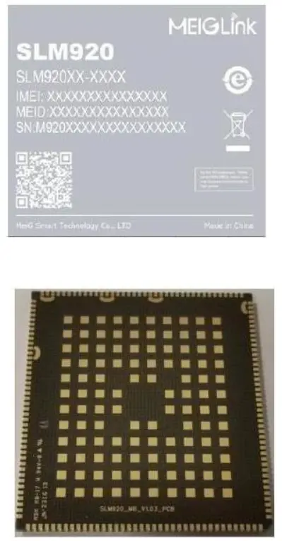 Foreword
Thank you for using the SLM920 module from Meg Smart. This product can provide data communication services. Please read the user manual carefully before use, you will appreciate its perfect function and simple operation method.
The company does not assume responsibility for property damage or personal injury caused by improper operation of the user. Users are requested to develop the corresponding products according to the technical specifications and reference designs in the manual. Also pay attention to the general safety issues that mobile products should focus on.
Before the announcement, the company has the right to modify the contents of this manual according to the needs of technological development.
Version History
Date | Version | Change description | Author |
| 2021-06 | 1.00 | First edition | Hardware Department |
| 2021-08 | 1.01 | 1. Updated the description of the USB interface hardware switching circuit 2. Updated PIN pin description, the GPIO suffix that supports interrupt function is marked with * | Hardware Department |
| 2022-08 | 1.02 | Update formatting and illustrations | Hardware Department |
| 2023-07 | 1.03 | Update the description of GPIO31 in Table 3.1 | Hardware Department |
Introduction
This document describes the hardware application interface of the module , including circuit connections and radio frequency interfaces in related applications . It can help users to quickly understand the detailed information of the module ‘s interface definition ,electrical performance and structural dimensions . Combined with this document and other application documents , users can quickly use the module to design mobile communication applications.
Module overview
SLM920 series core board, the main chip used is Qualcomm Snapdragon 600 series, the CPU is made of 11nm FinFET, built-in 64bit ARM, 8-core Kryo 260 CPU , the highest frequency is 2GHz.
SLM920 module is a broadband intelligent wireless communication module suitable for TD-LTE/FDD- LTE/WCDMA multiple network standards.
The working frequency bands supported by the SLM 920 module are (take China as an example) :
TDD-LTE:B41
FD D-LTE: B2/B4/B5/B7/B12/B13/B14/B17/B25/B26/B66
WCDMA: B2/B4/B5
GSM:850/1900MHz
SLM920 can provide voice, SMS, address book, WiFi, BT and GPS functions ; it can be widely used in VR Camera, intelligent robot, video surveillance, security, vehicle equipment, smart platform handheld terminal , etc.
The physical interface of the module is a 272 – pin pad, which provides the following hardware interfaces :
- Four 1.8V UART serial ports .
- One LCD interface (MIPI) .
- Three Camera interface (MIPI) .
- One flash interface.
- One USB interface (supports USB2.0 and USB3.1) .
- Three analog MIC input interface .
- Two digital MIC interfaces
- Three analog audio output interface (handset, earphone, AUX)
- Two (U)SIM card interface.
- 17 GPIO ports.
- Eight I2C interfaces .
- Two SPI interfaces.
- One TF card interface .
- Support GNSS , WiFi , Bluetooth 5.0 function .
- One ERM motor interface
- One I2S interface
Note: The number of functional interfaces is subject to the default function of the PIN
2.1. Main features of the module
Table 2.1 : Module main features
| Product Features | describe | |
| Platform | Qualcomm SM6125 | |
| CPU | Octa-core Kryo 260 CPU | |
| GPU | Adreno610® 950MHz | |
| System memory | 32GB eMMC + 3GB LPDDR 4X (default) 64GB eMMC + 4GB LPDDR 4X (optional) I6GB eMMC + 2GB LPDDR 4X (optional) I28GB UFS2.I + 6GB LPDDR 4X (optional) | |
| Operating system | Android 10 | |
| Size | 45.5×4 I .0x3.0mm. stamp hole package 160 pin+II2pin LCC+LGA | |
| Network frequency SLM920 | TDD-LTE: B41 FDD-LTE: B2/114/135/117/1112/B13/B14/B17/1325/1126/1366 WCDMA: B2/134/B5 GSM:850/1900 | |
| Wi-Fi | WCN3980: IEEE 802.11 a/ b/g/n /ac 2.4G &5G | |
| Bluetooth | BT 3.0/4.2/5.0 | |
| GNSS | GPS/Beidou/Glonass/Galileo | |
| Data access | TD-LTE | Cat4 TD-LTE 117/30Mbps |
| FDD-LTE | Cat4 FDD-LTE 150/50Mbps | |
| DC-HSPA+ TD-HSP | 42/11.2Mbps | |
| 2.8/2.3Mbps | ||
| EDGE | Class12, 236.8kbps/236.8kbps | |
| CPRS | Class12, 85.6kbps/85.6kbps | |
| SIM | DSD S Dual SIM Dual Standby ( 2.95V /1.8V ) Support SIM card hot swap L/W/G /T +G L/W/G /T + W L/W/G /T + 1X L /EVDO/CDMA1X+G Does not support dual CDMA cards | |
| Display | FHD+(2520X1080) 21:9@60fps | |
| LCD Size: User defined | ||
| Interface: 1st LCM: MIPI DSI 4-lane ; | ||
| Camera | Interface: Can support three groups of CSI, each group is 4-Lane | |
| (Dual cameras front and rear) | Dual 14 bit ISP 16+16MP, 25MP 30fps ZSL | |
| Video | Video decode | 4K30 8 bit: H.264/VP8 4K30 10bit: HEVC, VP9 1080P60 MPEG-2 |
| Video | Video encode | 4K30 10 bit: HEVC and 4K30 H.264/VP8 |
| Decode+Encode 4K30 | Buttons (power button, reset, Home, volume +, volume -) | |
| Input device | Capacitive TP | |
| Support hardware reset | ||
| Reset | ||
| Application interface | interface name | Main function description |
| VBAT | 2pin, module power input, 3.5V~4.2V, nominal value 3.8V | |
| SDIO *1 | SD3.0 | |
| USB2.0(3.1) | USB_BOOT (force USB boot, for emergency downloads) | |
| BLSP ports | 8 QUP ports | |
| ADC*2 | Suppor | |
| Charging function | Support QC 3.0 _ | |
| Motor | Support | |
| GPIO | 17 GPIOs ( excluding GPIOs involved in LCM TP CAMERA and GPIOs with specific functions) | |
| RE interface | Multimode LTE main antenna Multimode LTE Diversity Antenna GPS Antenna 2.4G WiFi /BT Antenna 5G WIFI-Antenna 3 analog MIC input | |
| Audio | 3 analog audio output interface (handset, earphone, AUX) 1 I2S interface 2 digital MIC interface | |
Module packaging
3.1. Pinout Diagram
Before PCB layout, we must first understand the pin distribution of the module, and rationally layout related devices and interfaces according to the distribution defined by the pins .
3.2. Module pin description
Table 3.1 : Pin description (GPIO with * supports interrupt function)
| PIN | pin name | GPIO | Attributes | Function description |
| 1 | GND | GND | GND | |
| 2 | FLASH_LED1+ | AO | Flash output positive (1.5A) | |
| 3 | GND | GND | GND | |
| 4 | PMI632_GPIO6_WLED_PWM | AI | ADC | |
| 5 | NC | Reserved PIN | ||
| 6 | NC | Reserved PIN | ||
| 7 | NC | Reserved PIN | ||
| 8 | VIB_DRV_LDO_N _ | GND | Motor drive negative, ground | |
| 9 | VIB_DRV_LDO_P | AO | Motor drive positive | |
| 10 | GND | GND | GND | |
| 11 | GPIO16_DEBUG_TX | GPIO_16 | B-PD: nppukp | Module debug serial port |
| 12 | GPIO17_DEBUG_RX | GPIO_17* | B-PD: nppukp | |
| 13 | GPIO4_APPS_I2C_SDA | GPIO_4* | B-PD: nppukp | General-purpose GPIO, used as I2C by default |
| 14 | GPIO5_APPS_I2C_SCL | GPIO_5 | B-PD: nppukp | |
| 15 | GPIO8_UART_TX | GPIO_8 | B-PD: nppukp | General-purpose GPIO, used as UART by default |
| 16 | GPIO9_UART_RX | GPIO_9* | B-PD: nppukp | |
| 17 | GPIO28_SENSOR_I2C_SDA | GPIO_28 | B-PD: nppukp | Dedicated for Sensor I2C |
| 18 | GPIO29_SENSOR_I2C_SCL | GPIO_29* | B-PD: nppukp | |
| 19 | GPIO80_ACCL_INT1 | GPIO_80* | B-PD: nppukp | Used as accelerometer interrupt by default |
| 20 | GPIO91_ALSP_INT_N | GPIO_91* | B-PD: nppukp | By default, it is used as a light distance sensor interrupt. |
| 21 | GPIO82_MAG_INT | GPIO_82* | B-PD: nppukp | By default it is used as a geomagnetic interrupt |
| 22 | GPIO81_GYRO_INT | GPIO_81* | B-PD: nppukp | Used as a gyro interrupt by default |
| 23 | GND | GND | GND | |
| 24 | KEY_VOLP_N | B-PD: nppukp | Volume up key | |
| 25 | GPIO26 | GPIO_26* | B-PD: nppukp | General purpose GPIO |
| 26 | GPIO27 | GPIO_27* | B-PD: nppukp | General purpose GPIO |
| 27 | GPIO116_I2S2_DATA1 | GPIO_116 | B-PD: nppukp | General-purpose GPIO, can be configured as I2S2_DATA1 |
| 28 | GND | GND | GND | |
| 29 | VREG_L22A_2P96 | PO | T card power supply | |
| 30 | VREG_L5A_2P96 | PO | T card signal pull-up power supply | |
| 31 | GPIO98_SDCARD_DET_N | GPIO_98* | B-PD: nppukp | T card hot plug detection signal |
| 32 | SDC2_SDCARD_D0 | BH-NP:pdpukp | T card data signal | |
| 33 | SDC2_SDCARD_D1 | BH-NP:pdpukp | ||
| 34 | SDC2_SDCARD_D2 | BH-NP:pdpukp | ||
| 35 | SDC2_SDCARD_D3 | BH-NP:pdpukp | ||
| 36 | SDC2_SDCARD_CMD | BH-NP:pdpukp | T card control signal | |
| 37 | SDC2_SDCARD_CLK | BH-NP:pdpukp | T card clock signal | |
| 38 | GND | GND | GND | |
| 39 | GND | GND | GND | |
| 40 | MIPI_CSI2_CLK_P | AI | MIPI-CSI2 differential clock signal | |
| 41 | MIPI_CSI2_CLK_N | AI |
| 42 | MIPI_CSI2_LANE0_P | AI | MIPI-CSI2 differential data signal | |
| 43 | MIPI_CSI2_LANE0_N | AI | ||
| 44 | MIPI_CSI2_LANE3_P | AI | ||
| 45 | MIPI_CSI2_LANE3_N | AI | ||
| 46 | MIPI_CSI2_LANE2_P | AI | ||
| 47 | MIPI_CSI2_LANE2_N | AI | ||
| 48 | GND | GND | GND | |
| 49 | MIPI_CSI0_CLK_P | AI | MIPI-CSI0 differential clock signal | |
| 50 | MIPI_CSI0_CLK_N | AI | ||
| 51 | MIPI_CSI0_LANE2_P | AI | MIPI-CSI0 differential data signal | |
| 52 | MIPI_CSI0_LANE2_N | AI | ||
| 53 | MIPI_CSI0_LANE3_P | AI | ||
| 54 | MIPI_CSI0_LANE3_N | AI | ||
| 55 | MIPI_CSI0_LANE0_P | AI | ||
| 56 | MIPI_CSI0_LANE0_N | AI | ||
| 57 | GND | GND | GND | |
| 58 | MIPI_CSI1_LANE1_P | AI | MIPI-CSI1 differential data signal | |
| 59 | MIPI_CSI1_LANE1_N | AI | ||
| 60 | MIPI_CSI1_LANE3_P | AI | ||
| 61 | MIPI_CSI1_LANE3_N | AI | ||
| 62 | MIPI_CSI1_LANE0_P | AI | ||
| 63 | MIPI_CSI1_LANE0_N | AI | ||
| 64 | MIPI_DSI0_CLK_N | AO | MIPI-DSI0 differential clock signal | |
| 65 | MIPI_DSI0_CLK_P | AO | ||
| 66 | MIPI_DSI0_LANE1_N | AO | MIPI-DSI0 differential data signal | |
| 67 | MIPI_DSI0_LANE1_P | AO | ||
| 68 | GND | GND | GND | |
| 69 | 5G_ANT | AI | 5G WIFI /BT antenna interface | |
| 70 | GND | GND | GND | |
| 71 | MIPI_DSI0_LANE2_N | AO | MIPI-DSI0 differential data signal | |
| 72 | MIPI_DSI0_LANE2_P | AO | ||
| 73 | MIPI_DSI0_LANE3_N | AO | ||
| 74 | MIPI_DSI0_LANE3_P | AO | ||
| 75 | GPIO90_LCD_RST_N | GPIO_90 | B-PD: nppukp | General-purpose GPIO, used as LCD reset signal by default |
| 76 | GPIO89_MDP_VSYNC_P | GPIO_89* | B-PD: nppukp | General-purpose GPIO, used as LCD frame synchronization signal by default |
| 77 | GPIO97 | GPIO_97* | B-PD: nppukp | General purpose GPIO |
| 78 | GPIO43_SCAM_PWD_N | GPIO_43* | B-PD: nppukp | General-purpose GPIO, used as proactive sleep signal by default |
| 79 | GPIO42_SCAM_RST_N | GPIO_42* | B-PD: nppukp | General-purpose GPIO, used as a proactive reset signal by default |
| 80 | GPIO36_CAM_MCLK2 | GPIO_36* | B-PD: nppukp | By default, it is used as the active master clock signal |
| 81 | GND | GND | GND | |
| 82 | WIFI_2.4G_ANT | AI | 2.4G WIFI interface | |
| 83 | GND | GND | GND | |
| 84 | GPIO34_CAM_MCLK0 | GPIO_34 | B-PD: nppukp | By default, it is used as the master clock signal for the rear camera. |
| 85 | GPIO48_MCAM_RST_N | GPIO_48 | B-PD: nppukp | General-purpose GPIO, used as the rear camera reset signal by default |
| 86 | GPIO49_MCAM_PWD_N | GPIO_49 | B-PD: nppukp | General-purpose GPIO, used as post-photo sleep signal by default |
| 87 | GPIO75_UIM2_DET | GPIO_75* | B-PD: nppukp | SIM card 1 hot plug detection signal |
| 88 | UIM2_RESET | GPIO_74 | B-PD: nppukp | SIM card 1 reset signal |
| 89 | UIM2_CLK | GPIO_73 | B-PD: nppukp | SIM card 1 clock signal |
| 90 | UIM2_DATA | GPIO_72* | B-PD: nppukp | SIM card 1 data signal |
| 91 | VREG_L20A_1P8 | PO | SIM card 1 power supply | |
| 92 | GND | GND | GND | |
| 93 | GPS_ANT | AI | GPS antenna interface | |
| 94 | GND | GND | GND | |
| 95 | CCI_I2C_SCL1 | GPIO_40 | B-PD: nppukp | Dedicated to camera I2C |
| 96 | CCI_I2C_SDA1 | GPIO_39 | B-PD: nppukp | |
| 97 | GPIO88_TP_INT_N | GPIO_88* | B-PD: nppukp | General-purpose GPIO, default for TP interrupt signal |
| 98 | GPIO87_TP_RST_N | GPIO_87 | B-PD: nppukp | General-purpose GPIO, used as TP reset signal by default |
| 99 | GPIO83 | GPIO_83* | B-PD: nppukp | General purpose GPIO |
| 100 | GPIO45 | GPIO_45* | B-PD: nppukp | General purpose GPIO |
| 101 | GND | GND | GND | |
| 102 | RF_DIV | AI | Diversity Antenna Interface | |
| 103 | GND | GND | GND | |
| 104 | CCI_I2C_SCL0 | GPIO_38 | B-PD: nppukp | Dedicated to camera I2C |
| 105 | CCI_I2C_SDA0 | GPIO_37 | B-PD: nppukp | |
| 106 | GPIO79_UIM1_DET | GPIO_79* | B-PD: nppukp | SIM card 0 hot plug detection signal |
| 107 | UIM1_RESET | GPIO_78 | B-PD: nppukp | SIM card 0 reset signal |
| 108 | UIM1_CLK | GPIO_77 | B-PD: nppukp | SIM 0 clock signal |
| 109 | UIM1_DATA | GPIO_76 | B-PD: nppukp | SIM card 0 data signal |
| 110 | VREG_L19A_1P8 | PO | SIM card 0 power | |
| 111 | GND | GND | GND | |
| 112 | PM6125_GPIO8_PWM | DO | PWM output | |
| 113 | VCOIN | AI, AO | RTC power supply | |
| 114 | WCD9370_AUX_M | AO | Class AB output, can be used as external PA input | |
| 115 | WCD9370_AUX_P | AO | ||
| 116 | GND | GND | GND | |
| 117 | MIC_BIAS3 | AO | MIC bias voltage | |
| 118 | MIC_BIAS1 | AO | ||
| 119 | GND | GND | GND | |
| 120 | RF_MAIN | AI | Main antenna interface | |
| 121 | GND | GND | GND | |
| 122 | MIC_IN1_P | AI | MIC1 differential input | |
| 123 | MIC_IN1_M | AI | ||
| 124 | MIC_IN3_M | AI | MIC3 differential input negative | |
| 125 | CDC_HS_DET | AI | Headphone plug-in detection signal | |
| 126 | CDC_HPH_L | AO | Headphone left channel | |
| 127 | CDC_HPH_REF | AI | Headphone Ground Reference | |
| 128 | CDC_HPH_R | AO | Headphone right channel | |
| 129 | CDC_EAR_M | AO | Earpiece differential output | |
| 130 | CDC_EAR_P | AO | ||
| 131 | MIC_IN3_P | AI | MIC3 differential input positive |
| 132 | MIC_IN2_P | AI | MIC2 single-ended input | |
| 133 | NC | Reserved PIN | ||
| 134 | NC | Reserved PIN | ||
| 135 | GND | GND | GND | |
| 136 | VREG_L21A_2P704 | PO | 2.8V power output, can be used for TP, LCD power supply | |
| 137 | VPH_PWR | PO | System power output, typical 3.8V | |
| 138 | VREG_L9A_1P8 | PO | 1.8V power output. Always supply when power on, used for signal pull-up | |
| 139 | VREG_L12A_1P8 | PO | 1.8V power output, always supply when power on, used for IO power supply | |
| 140 | VREG_L9A_1P8 | PO | 1.8V power output. Always supply when power on, used for signal pull-up | |
| 141 | PM_RESIN_N | DI | Module reset signal | |
| 142 | KYPD_PWR_N1 | DI | Module on/off signal | |
| 143 | GPIO131_USB_ID | GPIO_131* | DI | USB ID |
| 144 | GND | GND | GND | |
| 145 | USB_HS_DM | AI, AO | USB2.0 signal | |
| 146 | USB_HS_DP | AI, AO | ||
| 147 | GND | GND | GND | |
| 148 | BAT_CON_ID | AI | Battery ID detection signal | |
| 149 | BAT_THERM | AI | Battery temperature detection signal | |
| 150 | GND | GND | GND | |
| 151 | VBAT | PI,PO | Module power supply input, voltage range 3.5~4.2V, typical value 3.8V | |
| 152 | VBAT | PI,PO | ||
| 153 | VBAT_SNS_P | AI | Battery voltage detection differential signal | |
| 154 | VBAT_SNS_M | AI | ||
| 155 | GND | GND | GND | |
| 156 | GND | GND | GND | |
| 157 | VBUS | PI,PO | USB_VBUS | |
| 158 | VBUS | PI,PO | ||
| 159 | VBUS | PI,PO | ||
| 160 | GND | GND | GND | |
| 161 | GND | GND | GND | |
| 162 | USB3_SS_RX1_P | AI | USB3.1 channel 1 data receive differential signal | |
| 163 | USB3_SS_RX1_M | AI | ||
| 164 | GPIO14_I2C_SDA | GPIO_14* | B-PD: nppukp | Configurable GPIO, used as I2C by default |
| 165 | GPIO15_I2C_SCL | GPIO_15* | B-PD: nppukp | |
| 166 | GPIO84 | GPIO_84 | B-PD: nppukp | General purpose GPIO |
| 167 | GPIO85 | GPIO_85* | B-PD: nppukp | General purpose GPIO |
| 168 | GPIO93 | GPIO_93* | B-PD: nppukp | General purpose GPIO |
| 169 | GPIO113_I2S2_SCK | GPIO_113 | B-PD: nppukp | General-purpose GPIO, can be configured as I2S2_SCK |
| 170 | GND | GND | GND | |
| 171 | MIPI_CSI1_LANE2_P | AI | MIPI-CSI1 differential data signal | |
| 172 | MIPI_CSI1_LANE2_N | AI | ||
| 173 | USB3_SS_RX0_M | AI | USB3.1 channel 0 data receive differential signal | |
| 174 | USB3_SS_RX0_P | AI | ||
| 175 | GND | GND | GND | |
| 176 | GPIO24_UART_TX | GPIO_24 | B-PD: nppukp | General-purpose GPIO, used as UART by default |
| 177 | GPIO25_UART_RX | GPIO_25* | B-PD: nppukp | |
| 178 | USB3_SS_TX1_M | AO | USB3.1 channel 1 data transmission differential signal | |
| 179 | USB3_SS_TX1_P | AO | ||
| 180 | GND | GND | GND | |
| 181 | GND | GND | GND | |
| 182 | VREG_L15A_3P128 | PO | 3.128V power output for USB related chip power supply | |
| 183 | OPTION | DI | USB interface type switching signal | |
| 184 | GPIO22_I3C_SDA | GPIO_22* | B-PD: nppukp | General-purpose GPIO, used as I2C by default |
| 185 | GPIO23_I3C_SCL | GPIO_23 | B-PD: nppukp | |
| 186 | USB3_SS_TX0_P | AO | USB3.1 channel 0 data transmission differential signal | |
| 187 | USB3_SS_TX0_M | AO | ||
| 188 | USB_PHY_PS | GPIO_102* | DI | USB interface type switching signal |
| 189 | MIPI_DSI0_LANE0_N | AO | MIPI-DSI0 differential data signal | |
| 190 | MIPI_DSI0_LANE0_P | AO | ||
| 191 | MIPI_CSI2_LANE1_P | AI | MIPI-CSI2 differential data signal | |
| 192 | MIPI_CSI2_LANE1_N | AI | ||
| 193 | MIPI_CSI0_LANE1_P | AI | MIPI-CSI0 differential data signal | |
| 194 | MIPI_CSI0_LANE1_N | AI | ||
| 195 | GPIO128_DMIC_DAT2 | GPIO_128* | B-PD: nppukp | General-purpose GPIO, configurable as a digital MIC interface |
| 196 | GPIO127_DMIC_CLK2 | GPIO_127 | B-PD: nppukp | |
| 197 | GPIO101_WSA_EN | GPIO_101* | B-PD: nppukp | General purpose GPIO |
| 198 | GPIO124_WSA_INT | GPIO_124* | B-PD: nppukp | General purpose GPIO |
| 199 | NC | Reserved PIN | ||
| 200 | NC | Reserved PIN | ||
| 201 | PMI632_USB_CC1 | I/O | Type-C configuration channel 1 | |
| 202 | PMI632_USB_CC2 | I/O | Type-C configuration channel 2 | |
| 203 | CBL_PWR_N1 | DI | Module power-on automatic power-on signal | |
| 204 | GPIO125_DMIC_CLK1 | GPIO_125 | B-PD: nppukp | General-purpose GPIO, configurable as a digital MIC interface |
| 205 | GPIO126_DMIC_DAT1 | GPIO_126* | B-PD: nppukp | |
| 206 | FORCE_USB_BOOT | GPIO_99* | DI | Emergency download mode interface |
| 207 | MIPI_CSI1_CLK_N | AI | MIPI-CSI1 differential clock signal | |
| 208 | MIPI_CSI1_CLK_P | AI | ||
| 209 | PM6125_GPIO3_ADC | AI | ADC | |
| 210 | GND | GND | GND | |
| 211 | GND | GND | GND | |
| 212 | GPIO86 | GPIO_86* | B-PD: nppukp | General purpose GPIO |
| 213 | GND | GND | GND | |
| 214 | GND | GND | GND | |
| 215 | GND | GND | GND | |
| 216 | GND | GND | GND | |
| 217 | NC | Reserved PIN | ||
| 218 | GND | GND | GND | |
| 219 | NC | Reserved PIN | ||
| 220 | GND | GND | GND | |
| 221 | GPIO94_PRESSURE_INT | GPIO_94* | B-PD: nppukp | General purpose GPIO |
| 222 | GND | GND | GND | |
| 223 | GND | GND | GND |
| 224 | GND | GND | GND | |
| 225 | NC | Reserved PIN | ||
| 226 | NC | Reserved PIN | ||
| 227 | NC | Reserved PIN | ||
| 228 | GPIO117_WCD_ELDO_EN | GPIO_117 | B-PD: nppukp | General purpose GPIO |
| 229 | USB0_DP_AUX_C_M | AO, AI | DP auxiliary channel differential signal | |
| 230 | USB0_DP_AUX_C_P | AO, AI | ||
| 231 | GPIO100 | GPIO_100* | B-PD: nppukp | General purpose GPIO |
| 232 | GPIO119 | GPIO_119 | B-PD: nppukp | General purpose GPIO |
| 233 | GPIO7_TS_I2C_SCL | GPIO_7 | B-PD: nppukp | General-purpose GPIO, configured as TP I2C by default |
| 234 | GPIO6_TS_I2C_SDA | GPIO_6 | B-PD: nppukp | |
| 235 | PM6125_GPIO2 | B-PD: nppukp | General purpose GPIO | |
| 236 | NC | Reserved PIN | ||
| 237 | NC | Reserved PIN | ||
| 238 | NC | Reserved PIN | ||
| 239 | NC | Reserved PIN | ||
| 240 | NC | Reserved PIN | ||
| 241 | MIPI_DSI1_CLK_P | AO | MIPI-DSI1 differential clock signal | |
| 242 | MIPI_DSI1_CLK_N | AO | ||
| 243 | NC | Reserved PIN | ||
| 244 | NC | Reserved PIN | ||
| 245 | NC | Reserved PIN | ||
| 246 | NC | Reserved PIN | ||
| 247 | PM6125_GPIO1 | B-PD: nppukp | General purpose GPIO | |
| 248 | GPIO123 | GPIO_123* | B-PD: nppukp | General purpose GPIO |
| 249 | GPIO41 | GPIO_41 | B-PD: nppukp | General purpose GPIO |
| 250 | CC_OUT | DO | USB interface type switching signal | |
| 251 | GPIO130 | GPIO_130* | B-PD: nppukp | General purpose GPIO |
| 252 | GND | GND | GND | |
| 253 | GPIO1_I2C_SCL | GPIO_1* | B-PD: nppukp | General purpose GPIO, configurable as I2C |
| 254 | GPIO0_I2C_SDA | GPIO_0 | B-PD: nppukp | |
| 255 | GPIO3_UART_RX | GPIO_3* | B-PD: nppukp | General purpose GPIO, configurable as UART |
| 256 | GPIO2_UART_TX | GPIO_2 | B-PD: nppukp | |
| 257 | GND | GND | GND | |
| 258 | GPIO20_SPI_CLK | GPIO_20 | B-PD: nppukp | General purpose GPIO, configurable as SPI |
| 259 | GPIO21_SPI_CS | GPIO_21* | B-PD: nppukp | |
| 260 | GPIO18_SPI_MISO | GPIO_18 | B-PD: nppukp | |
| 261 | GPIO19_SPI_MOSI | GPIO_19* | B-PD: nppukp | |
| 262 | GPIO44_DCAM_PWD_N | GPIO_44* | B-PD: nppukp | General-purpose GPIO, used as the sleep signal of the depth-of-field camera by default |
| 263 | GPIO46_DCAM_RST_N | GPIO_46 | B-PD: nppukp | General-purpose GPIO, used as depth camera reset signal by default |
| 264 | GPIO35_CAM_MCLK1 | GPIO_35 | B-PD: nppukp | General-purpose GPIO, used as the main clock signal of the depth camera by default |
| 265 | GPIO115_I2S2_DATA0 | GPIO_115 | B-PD: nppukp | General-purpose GPIO, can be configured as I2S2_DATA0 |
| 266 | GPIO30_SPI_MISO | GPIO_30 | B-PD: nppukp | General purpose GPIO, configurable as SPI |
| 267 | GPIO31_SPI_MOSI | GPIO_31 | B-PD: nppukp | |
| 268 | GPIO33_SPI_CS | GPIO_33* | B-PD: nppukp |
| 269 | GPIO32_SPI_CLK | GPIO_32 | B-PD: nppukp | |
| 270 | GPIO92_FP_INT_N | GPIO_92* | B-PD: nppukp | General purpose GPIO |
| 271 | GPIO114_I2S2_WS | GPIO_114 | B-PD: nppukp | General-purpose GPIO, configurable as I2S2_WS |
| 272 | GND | GND | GND |
Note:
* : Interrupt pin that can wake up the system
B:Bidirectionaldigital with CMOS input
H:High-voltage tolerant
NP:pdpukp=defaultno-pull with programmable options following the colon (:)
PD:nppukp=defaultpulldown with programmable options following the colon (:)
PU:nppdkp=defaultpullup with programmable options following the colon (:)
KP:nppdpu=defaultkeeper with programmable options following the colon (:)
3.3. Mechanical Dimensions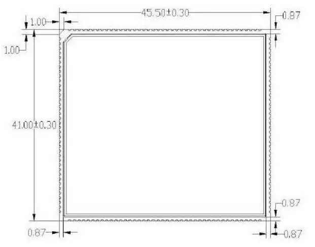
Interface application
4.1. Power supply
If it is a device with battery, the voltage input range of module VBAT is 3.5 V to 4.2 V, and the recommended voltage is 3.8 V. In the GSM frequency band, when the module transmits at the maximum power, the peak current can reach up to 3 A instantaneously, resulting in a large voltage drop on VBAT.
It is recommended to use a large capacitor for voltage regulation close to VBAT. It is recommended to use two 47uF ceramic capacitors. Parallel 33PF and 10PF capacitors can effectively remove high frequency interference. At the same time, in order to prevent ESD and surge damage to the chip, it is recommended to use a suitable TVS tube and a 5.1 V /500mW Zener diode on the VBAT pin of the module. During PCB layout, capacitors and diodes should be placed as close as possible to the VBAT pin of the module. Users can directly supply power to the module with a 3.8 V lithiumion battery. When using a battery, the impedance between the VBAT pin and the battery should be less than 150mΩ. If it is a DC power supply device, the DC input voltage is 5V -12V , and the recommended circuit that can use DC-DC power supply at this time is shown in the figure below :
  Notice:
If the user does not use the battery for power supply, VBAT_SNS_P /M can not be left floating. It is necessary to connect VBAT_SNS_P to VBAT and VBAT_SNS_M to ground. Pin 149 (BAT_THERM) of the module is connected to a 10K resistor and pulled down to GND to prevent the software from judging that the battery temperature is abnormal after the module is turned on, resulting in shutdown. The connection diagram is as follows :  4.1.1. Power supply pins
VBAT pins ( 151 , 152 ) are used for power input. In the user’s design, please pay special attention to the design of the power supply part to ensure that even when the current consumption of the module reaches 3 A, the drop of VBAT will not be lower than 3.5 V . If the voltage drops below 3.5 V , the module may shut down . The PCB trace from the VBAT pin to the power supply should be wide enough to reduce voltage droop during transmission burst mode. 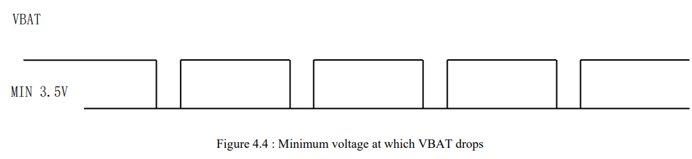 4.1.2. Power PCB Layout
The power trace should not only consider VBAT, but also the return GND of the power supply. The trace of the positive pole of VBAT must be short and thick, and the trace must first pass through a large capacitor, a Zener diode, and then to the power PIN of the module. There are multiple PAD exposed coppers at the bottom of the module. It is necessary to ensure that the GND path from these exposed copper areas to the power supply is the shortest and most unobstructed. In this way, the current path of the entire power supply can be guaranteed to be the shortest and the interference can be minimized.
4.2. Power on and off
Do not turn on the module when the temperature and voltage limits of the module are exceeded. In extreme cases such operations can lead to permanent damage to the module.
4.2.1. Module power on
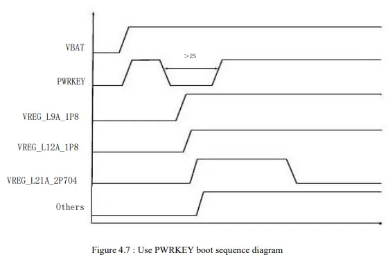
by pulling down the KYPD_PWR_N1 pin ( 142 ) for at least 2 seconds . This pin has been pulled up to 1.8V in the module. The recommended circuit is as follows ; or pull down the CBL_PWR_N pin (203), CBL_PWR_N can realize the function of automatic power-on after power-on by means of a 1K pull-down resistor to GND, and it is not necessary to release this signal after power-on. 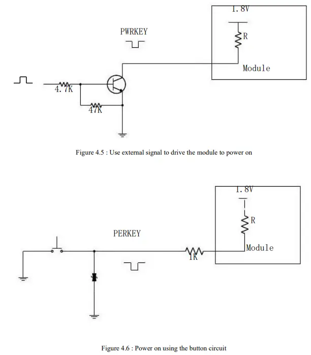
 4.2.2. Module shutdown
User can shutdown using PWRKEY pin
4.2.2.1. PWRKEY shutdown
The user can shut down by pulling the PWRKEY signal low for at least 3 seconds. The shutdown circuit can refer to the design of the startup circuit. After the module detects the shutdown action, a prompt window will pop up on the screen to confirm whether to perform the shutdown action. restart by pulling down PWRKEY for at least 15 seconds.
4.2.3. Module reset
SLM920 module supports the reset function, and the user can quickly restart the module by pulling down the PM_RESIN_N (PIN141) pin of the module. The recommended circuit is as follows: 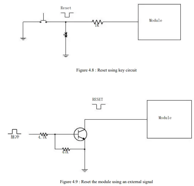 When the pin is at a high level, the voltage is typically 1.8V, so users with a level of 3V or 3.3V cannot directly use the GPIO of the MCU to drive this pin, and a voltage conversion circuit needs to be added. The hardware parameters of RESET can refer to the following table :
Table 4.1 : RESET Hardware Parameters
| Pin | Describe | Minimum | Typical value | Maximu m value | Unit |
| PM_RESIN_N | Input high level | 1.4 _ | 1.8 | – | V |
| Input low level | – | 0 | 0.6 | V | |
| Pull down valid time | 500 | – | ms |
4.3. VCOIN power supply
When the VBAT is disconnected, the user needs to save the real-time clock, so the VCOIN (113) pin cannot be left floating, and should be connected to a large capacitor or a button battery. When an external large capacitor is connected, the recommended value is 100 uF. When the RTC power supply uses an external large capacitor or battery to supply power to the RTC inside the module, the reference design circuit is as follows: 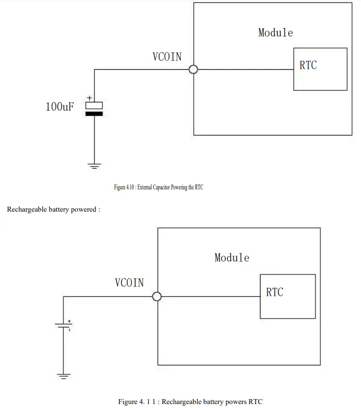 The VCOIN power supply input voltage range is 2.5-3.1V, the typical value is 3.0V, and the current consumption is about 20 uA when VBAT is disconnected.
4.4. Power output
The SLM920 has multiple power outputs. For SD card, SIM card , Sensor , Touch panel , USB3.1 circuit, external LDO power supply , etc. In application, it is recommended to add parallel 33PF and 10PF capacitors to each power supply to effectively remove high-frequency interference.
Table 4.2 : Power Supply Description
| Signal | Programmable Range ( V ) | Default voltage (V) | Drive current (mA) |
| VREG_L22A_2P96 | 1.504–3.544 | 2.96 | 600 |
| VREG_L5A_2P96 | 1.504–3.544 | 2.96 | 50 |
| VREG_L20A_1P8 | 1.504–3.544 | 1.8 | 100 |
| VREG_L19A_1P8 | 1.504–3.544 | 1.8 | 100 |
| VREG_L21A_2P704 | 1.504–3.544 | 2.8 | 300 |
| VREG_L9A_1P8 | 1.504–2.000 | 1.8 | 100 |
| VREG_L12A_1P8 | 1.504–2.000 | 1.8 | 200 |
| VREG_L15A_3P128 | 1.504–3.544 | 3.128 | 100 |
| VPH_PWR | Variation with VBAT voltage | 3.8 | 700 |
4.5. Serial port
SLM920 provides four serial ports for communication.
Table 4.3 : UART pin descriptions
| Name | Pin | Direction | Function |
| GPIO16_DEBUG_TX | 11 | DO | DEBUG UART data transmission |
| GPIO17_DEBUG_RX | 12 | DI | DEBUG UART data reception |
| GPIO9_UART_RX | 16 | DI | UART data reception |
| GPIO8_UART_TX | 15 | DO | UART data transmission |
| GPIO24_UART_TX | 176 | DO | UART data transmission |
| GPIO25_UART_RX | 177 | DI | UART data reception |
| GPIO2_UART_TX | 256 | DO | UART data transmission |
| GPIO3_UART_RX | 255 | DI | UART data reception |
If you need to use a four-wire serial port, you can refer to the GPIO multiplexing table for multiplexing.
For serial connection , please refer to the connection method below :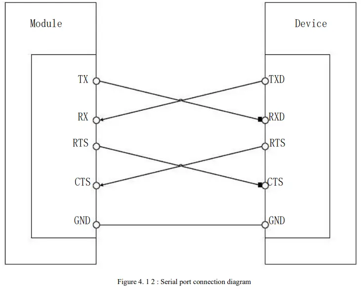 When the level of the serial port used by the user does not match the module, in addition to adding a level conversion IC, the following figure can also be used to achieve level matching. Only the matching circuits on TX and RX are listed here. Other low-speed signals can refer to this two circuits.
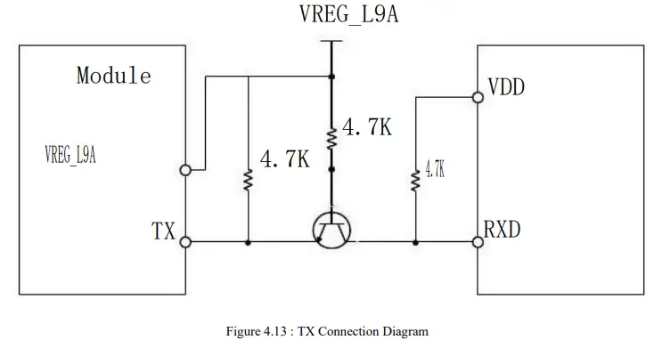
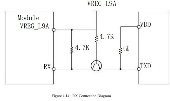 Note: When using Figure 4.13 and 4.14 for level isolation, it is recommended to use VREG_L9A_1P8 as the pull-up power supply.
Table 4.4 : Serial hardware parameters
| Describe | Minimum | Maximum value | Unit |
| Input low level | – | 0.63 | V |
| Input high level | 1.17 | – | V |
| Output low level | – | 0.45 | V |
| Output high level | 1.35 | – | V |
Note:
- The serial port of the module is a CMOS interface and cannot be directly connected to RS232 signals. If needed, please use RS232 conversion chip.
- If the 1.8V output of the module cannot meet the high level range of the user, please add a level conversion circuit.
4.6. MIPI interface
SLM920 supports MIPI interface for Camera and LCD.
MIPI is a high-speed signal line. In the layout stage, please strictly follow the impedance and length requirements , control the equal length of the differential pair within the group and between the groups, and keep the total length as short as possible.
4.6.1. LCD interface
SLM920 module supports the MIPI interface of 1 group of LCD display screen, and the resolution of the screen can be up to FHD+ (2520X1080) . The signal interface is shown in the table below. During layout, please strictly control the differential 85 ± 15 Ω impedance of the MIPI signal line and the equal length of the signal line within and between groups .
The MIPI interface of the module is 1.2V power domain. When the user needs to be compatible with the screen design, the LCD_ID pin or ADC pin of the module can be used. The LCD interface is as follows:
Table 4.5 : Screen Interface Definition
| Screen interface | |||
| MIPI_DSI0_CLK_N | 64 | AO | MIPI_LCD clock line |
| MIPI_DSI0_CLK_P | 65 | AO | |
| MIPI_DSI0_LANE0_N | 189 | AO | MIPI_LCD data line |
| MIPI_DSI0_LANE0_P | 190 | AO | |
| MIPI_DSI0_LANE1_N | 66 | AO | |
| MIPI_DSI0_LANE1_P | 67 | AO | |
| MIPI_DSI0_LANE3_N | 73 | AO | |
| MIPI_DSI0_LANE3_P | 74 | AO | |
| MIPI_DSI0_LANE2_N | 71 | AO | |
| MIPI_DSI0_LANE2_P | 72 | AO | |
| GPIO90_LCD_RST_N | 75 | I/O | LCD reset pin |
| GPIO89_MDP_VSYNC_P | 76 | I/O | LCD frame sync signal |
| PM6125_GPIO8_PWM | 112 | I/O | Screen backlight PWM control |
| VREG_L9A_1P8 | 138,140 | PO | 1.8V power supply |
| VREG_L21A_2P704 | 2.8V power output | PO | 2.8V power supply |
When the customer needs a compatible screen design, the LCD_ID pin of the LCD should be connected to the ADC of the module, but it should be noted that the output voltage of the LCD_ID cannot exceed the ADC pin voltage range.
MIPI is a high-speed signal line. To avoid EMI interference, it is recommended to place a common mode inductor on the side close to the LCD.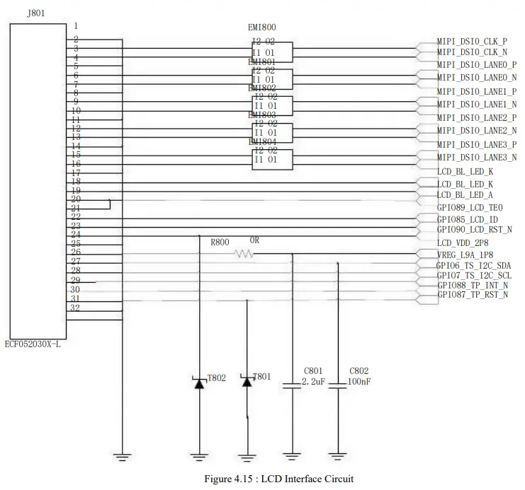 SLM920 module does not support backlight driver output, customers need to use external backlight driver.
The backlight drive circuit can refer to Figure 4.16. The backlight brightness can be adjusted through PM6125_GPIO8_PWM (112) of the module , and the modulation mode is PWM mode.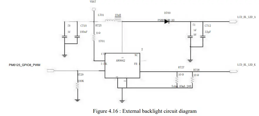 Note: 1. The backlight circuit should select the chip according to the backlight circuit of the LCD, and the user should read the LCD documentation carefully and select the correct driver chip. The reference circuit provided in this document is a series-type PWM dimming backlight drive circuit ; if it is a series-type one-line dimming backlight drive circuit, it needs to be controlled by GPIO.
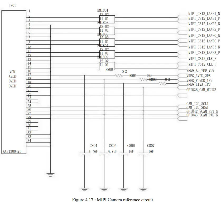
4.6.2. MIPI Camera interface
SLM920 module supports MIPI interface Camera. Rear camera is CSI0 interface, supports four groups of data lines, and can support up to 25M pixels. Front camera is a CSI2 interface, supports four sets of data lines, and can support 16M pixels. There is also a set of CSI1 interfaces, which can be used as a dual 16M dual-camera design with the Rear camera, or as a dual-camera design for a depth-of-field camera; it can also be used as a MIPI interface scan head design. The power required by the Camera, including AVDD-2.8V , AFVDD-2.8V and DVDD- 1.2V, needs to be provided by an external LDO.
Table 4.6 : MIPI Camera Interface Definition
| Main camera interface | |||
| Name | Pin | Input Output | Describe |
| MIPI_CSI0_CLK_N | 50 | AI/AO | MIPI clock signal of the main camera |
| MIPI_CSI0_CLK_P | 49 | AI/AO | |
| MIPI_CSI0_LANE0_N | 56 | AI/AO | MIPI data signal of the main camera |
| MIPI_CSI0_LANE0_P | 55 | AI/AO | |
| MIPI_CSI0_LANE1_N | 194 | AI/AO | |
| MIPI_CSI0_LANE1_P | 193 | AI/AO | |
| MIPI_CSI0_LANE2_N | 52 | AI/AO | |
| MIPI_CSI0_LANE2_P | 51 | AI/AO | |
| MIPI_CSI0_LANE3_N | 54 | AI/AO | |
| MIPI_CSI0_LANE3_P | 53 | AI/AO | |
| GPIO32_CAM_MCLK0 | 84 | I/O | Main camera clock signal |
| GPIO46_CAM0_RST_N | 85 | I/O | Main camera reset signal |
| GPIO49_MCAM_PWD_N | 86 | I/O | Main camera sleep signal |
| CCI_I2C_SCL0 | 105 | I/O | I2C data |
| CCI_I2C_SCL0 | 104 | I/O | I2C clock |
| VREG_L12A_1P8 | 139 | PO | 1.8V IOVDD |
| MIPI_CSI2_LANE3_P | 44 | AI/AO | |
| MIPI_CSI2_LANE3_N | 45 | AI/AO | |
| GPIO36_CAM_MCLK2 | 80 | I/O | Front camera clock signal |
| GPIO42_SCAM_RST_N | 79 | I/O | Front camera reset signal |
| GPIO43_SCAM_PWD_N | 78 | I/O | Front camera sleep signal |
| CCI_I2C_SDA1 | 96 | I/O | I2C data |
| CCI_I2C_SCL1 | 95 | I/O | I2C clock |
| VREG_L12A_1P8 | 139 | PO | 1.8V IOVDD |
Front camera interface
| Name | Pin | Input Output | Describe |
| MIPI_CSI2_CLK_P | 40 | AI/AO | |
| MIPI_CSI2_CLK_N | 41 | AI/AO | MIPI clock signal of the front camera |
| MIPI_CSI2_LANE0_P | 42 | AI/AO | |
| MIPI_CSI2_LANE0_N | 43 | AI/AO | |
| MIPI_CSI2_LANE1_P | 191 | AI/AO | |
| MIPI_CSI2_LANE1_N | 192 | AI/AO | MIPI data signal of front camera |
| MIPI_CSI2_LANE2_P | 46 | AI/AO | |
| MIPI_CSI2_LANE2_N | 47 | AI/AO |
Depth of Field Camera Interface
| Name | Pin | Input Output | Describe |
| MIPI_CSI1_CLK_N | 207 | AI/AO | MIPI clock signal of Depth camera |
| MIPI_CSI1_CLK_P | 208 | AI/AO | |
| MIPI_CSI1_LANE0_N | 63 | AI/AO | MIPI data signal of Depth camera |
| MIPI_CSI1_LANE0_P | 62 | AI/AO | |
| MIPI_CSI1_LANE1_N | 59 | AI/AO | |
| MIPI_CSI1_LANE1_P | 58 | AI/AO | |
| MIPI_CSI1_LANE2_N | 172 | AI/AO | |
| MIPI_CSI1_LANE2_P | 171 | AI/AO | |
| MIPI_CSI1_LANE3_N | 61 | AI/AO | |
| MIPI_CSI1_LANE3_P | 60 | AI/AO | |
| GPIO35_CAM_MCLK1 | 264 | I/O | Depth camera clock signal |
| GPIO46_DCAM_RST_N | 263 | I/O | Depth camera reset signal |
| GPIO44_DCAM_PWD_N | 262 | I/O | Depth camera sleep signal |
| CCI_I2C_SDA1 | 96 | I/O | I2C data |
| CCI_I2C_SCL1 | 95 | I/O | I2C clock |
| VREG_L12A_1P8 | 139 | PO | 1.8V IOVDD |
The MIPI interface speed is relatively high. Users should control the impedance according to 85 ± 1 5 Ω in the routing stage . At the same time, please pay attention to the requirements of the trace length. It is not recommended to add small capacitors on the MIPI signal line, which may affect the rise of MIPI data. edge time, which in turn results in invalid MIPI data.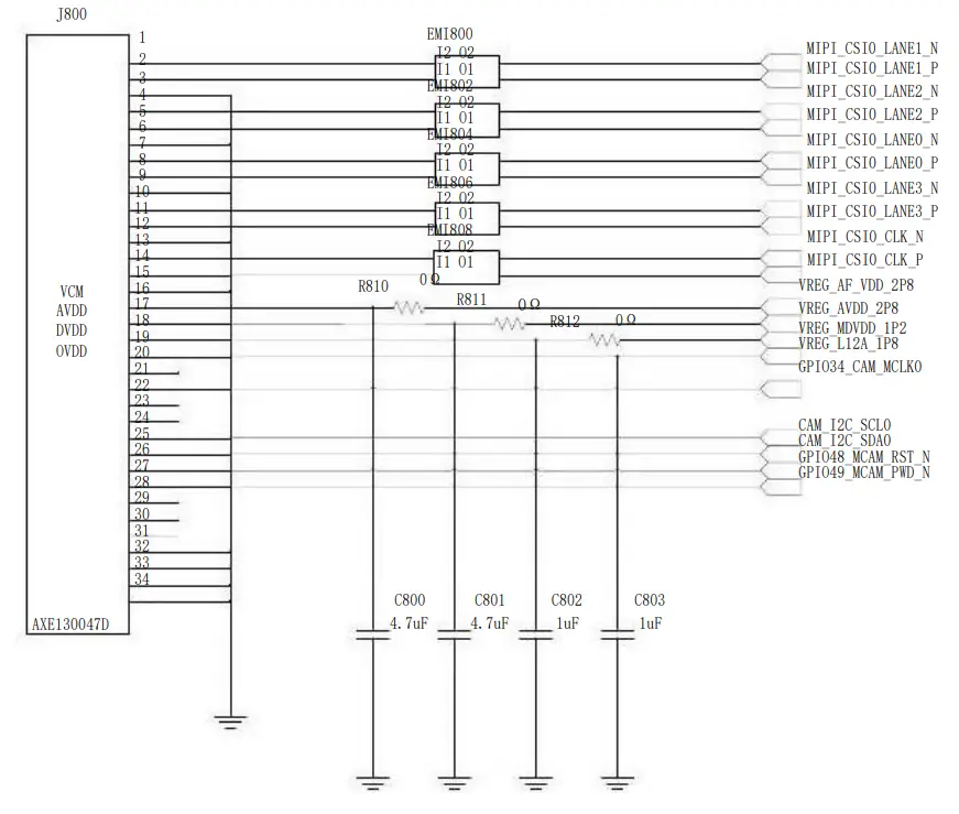
 4.6.3. MIPI PCB Layout
MIPI is a high-speed signal line. The user must pay attention to protection during the layout stage to keep it away from the signal line that is easily disturbed. It must be processed with GND on the top, bottom, left , and right . To ensure the consistency of impedance, try not to bridge different GND planes.
When choosing an ESD device for the MIPI interface, please choose a TVS with a small capacitance value. It is recommended that the parasitic capacitance be less than 1pF.
MIPI routing requirements are as follows:
- The total length of the traces shall not exceed 300 mm
- Requires control of 85 ohm differential impedance with an error of ±15 ohms .
- The length error of the differential line within the group is controlled within 0.7 mm.
- The length error between groups was controlled within 1.4 mm.
4.7. Capacitive touch interface
The module provides a set of I2C interfaces that can be used to connect capacitive touch, as well as the required power supply and interrupt pins. The default interface pins of the capacitive touch software are defined in the following table:
Table 4.7: Capacitive Touch Interface Definition
| Name | Pin | Input / output | Describe |
| GPIO6_TS_I2C_SDA | 234 | I/O | I2C interface of TP |
| GPIO7_TS_I2C_SCL | 233 | I/O | |
| GPIO67_TP_INT_N | 97 | I/O | TP interrupt |
| GPIO66_TP_RST_N | 98 | I/O | TP reset |
Note: The interface definition of capacitive touch can be adjusted by software, and users can change GPIO and I2C according to design needs.
4.8. Audio interface
Module provides three analog audio inputs , MIC_IN1_P /M is used to connect the main microphone;
MIC_IN2 _P can be used to connect the headphone microphone , and MIC_IN3 _P /M is used to connect the noise reduction microphone . The module also provides three analog audio outputs (CDC_HPH_L/R, CDC_EAR_P/M , WCD9370_AUX_P/M ), and the audio pins are defined as follows:
Table 4.8: Audio pin definition
Name | Pin | Input/Output | Describe |
| MIC_IN1_M | 123 | AI | MIC1 differential input |
| MIC_IN1_P | 122 | AI | |
| MIC_IN2_P | 132 | AI | MIC2 single-ended input |
| MIC_IN3_M | 124 | AI | MIC3 differential input |
| MIC_IN3_P | 131 | AI | |
| MIC_BIAS1 | 118 | AO | MIC bias voltage |
| MIC_BIAS3 | 117 | AO | |
| CDC_HPH_R | 128 | AO | Headphone right channel |
| CDC_HPH_L | 126 | AO | Headphone left channel |
| CDC_HS_DET | 125 | DI | Headphone plug-in detection |
| CDC_HPH_REF | 127 | AI | Headphone Ground Reference |
| CDC_EAR_M | 129 | AO | Earpiece differential output |
| CDC_EAR_P | 130 | AO | |
| WCD9370_AUX_M | 114 | AO | Class AB output, can be used as external PA input |
| WCD9370_AUX_P | 115 | AO |
It is recommended that the user choose the following circuit according to the actual application to get better sound effect.
4.8.1. The handset interface circuit
The receiver interface circuit places the following devices near the REC end, B302 and B303 can be changed to magnetic beads according to the actual effect.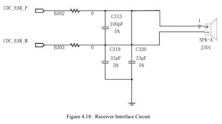 4.8.2. Microphone receiving circuit
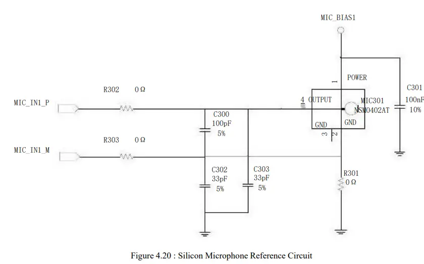
The following figures are the electret microphone (ECM) reference circuit and the analog silicon microphone (MEMS) reference circuit. 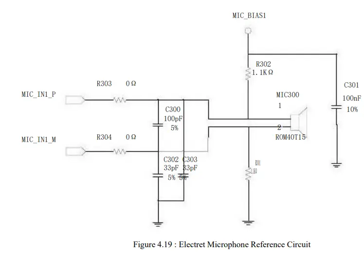
 4.8.3. Headphone interface circuit
The module integrates a stereo headphone jack. It is recommended that users reserve ESD devices in the design stage to prevent ESD damage. The CDC_HS_DET pin of the module can be set as an interrupt. The software defaults to this pin as a headset interrupt, and the user can use this pin to detect the plugging and unplugging of the headset.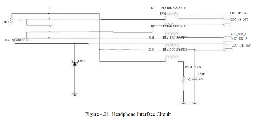 Notice:
- The headphone holder in Figure 4.21 is normally closed. If the user uses the normally open headphone holder, please modify the detection circuit according to the actual pins and modify the software accordingly.
- We recommend that the headphone detection pins CDC_HS_DET and CDC_HPH_L form a detection circuit (the connection method in the above figure), because CDC_HPH_L has a pull-down resistor inside the chip , which can ensure that CDC_HS_DET and CDC_HPH_L are connected to a low level, if The user connects CDC_HS_DET with CDC_HPH_R , please reserve the position of 1K pull-down resistor on HPH_R.
- The standard of the headphone jack shown in the figure is the European standard OMPT. If you need to design the American standard CTIA interface, you need to exchange the GND and MIC signals for the network. If you want to be compatible with two headset standards, you need an external dedicated chip, such as TI-TS3A226AE.
4.8.4. Speaker interface circuit
WCD9370_AUX_P/M output by the module needs an external audio PA to effectively drive the speaker. The reference circuit is shown in the figure below. 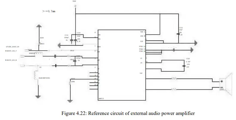 4.8.5. I2S interface
There is a set of GPIO compatible I2S interface inside the module . The pins used by this function are as follows:
| name | pin | input / output | describe |
| GPIO115_I2S2_DATA0 | 265 | I/O | I2S data channel 0 |
| GPIO116_I2S2_DATA1 | 27 | I/O | I2S data channel 1 |
| GPIO114_I2S2_WS | 271 | I/O | I2S channel selection |
| GPIO113_I2S2_SCK | 169 | I/O | I2S serial clock |
4.8.6. Audio PCB Layout
The module supports 3 channels of analog audio signals. Analog signals are susceptible to interference from high-speed digital signals. So please stay away from high-speed digital signal lines. The module supports the GSM standard, and the GSM signal can interfere with the audio through coupling and conduction. Users can add 33pF and 10pF capacitors to the audio path to filter out coupling interference. The 33pF capacitor mainly filters out the interference in the GSM850/EGSM900 frequency band, and the 10pF capacitor mainly filters out the interference in the DCS1800 frequency band. The coupling interference of TDD has a lot to do with the user’s PCB design. In some cases, the TDD in the GSM850/EGSM900 frequency band is more serious, and in some cases the TDD interference in the DCS1800 frequency band is serious. Therefore, users can select the required filter capacitors according to the actual test results, and sometimes even do not need to paste filter capacitors.
The GSM antenna is the main source of coupling interference for TDD, so users should pay attention to keeping the audio traces away from the GSM antenna and VBAT during PCB layout and routing. It is best to place a set of audio filter capacitors close to the module end, and another set close to the interface end. The audio output should be routed according to the differential signal rules.
The conducted interference is mainly caused by the voltage drop of VBAT. If the Audio PA is directly powered by VBAT, it is easier to hear the “squeak” sound at the output end of the SPK, so it is best to connect the input end of the Audio PA in parallel in the schematic design. Some bulk capacitors and ferrite beads in series. TDD and GND are also closely related. If the GND is not handled properly, many high-frequency interference signals will interfere with the MIC and Speaker through bypass capacitors and other devices.
Therefore, the user should ensure the good performance of the GND during the PCB design stage.
4.9. USB interface
SLM920 supports one USB 2.0 interface and one USB 3.1 interface. During layout, it is necessary to control 90 ohm differential impedance and control the length of external traces.
The module also supports OTG function and can output 5V/1A current.
VBUS voltage input range is as follows:
Table 4.9: VBUS voltage input range
| Name | Describe | Minimum | Typical | Maximum | Unit |
| VBUS | input range | 3.6 | 5 | 10 | V |
The USB insertion detection of the module is realized by VBUS and DP/DM data line . When the USB line is inserted, the VBUS voltage is detected first, and then the up-down state of the DM/DP is detected to determine whether the USB data line or the charger is inserted . Therefore, if the user needs to use the USB function, please be sure to connect VBUS to the 5V power supply on the data line.
USB is in high-speed mode. It is recommended to connect a common mode inductor in series near the USB connector, which can effectively suppress EMI interference. At the same time, the USB interface is an external interface, and DM/DP must add a TVS tube to prevent electrostatic damage caused by plugging and unplugging the data cable. When choosing TVS, users should pay attention to the load capacitance should be less than 1pf. VBUS also needs to increase the TVS tube, if there is a need for anti-surge, but also add a surge-proof tube. The connection diagram is as follows: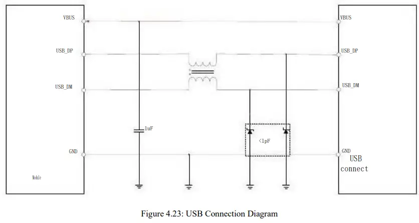 SLM920 provides three pins for hardware switching between Micro-USB and Type-C interfaces. The interface definitions are as follows:
| Pin name | Pin number | Function description | Note |
| USB_PHY_PS | 188 | USB PHY port selection | Connect 10K resistor to ground, the default is Micro USB mode, connect to CC_OUT, the default is Type-C mode |
| OPTION | 183 | Select different PON options based on pull- down resistor value | Connect 1k resistor to ground, default is Mirco USB mode, connect 1M resistor to ground, default is Type-C mode |
| CC_OUT | 250 | 1.8V push-pull 3-state output, indicating CC1 or CC2 connection |
Note: The CC pin of SLM920 does not support the PD protocol. If the customer needs the CC pin to support the PD protocol, an external CC logic chip is required. In this case, the interface switching circuit can only be fixed in Micro-USB mode.
4.9.1. USB OTG
SLM920 module can provide USB -OTG function, the pins used by this function are as follows:
Table 4.10: USB-OTG pin description
| Pin name | Pin | Describe |
| VBUS | 157, 158, 159 | 5V charging input/OTG output power supply. |
| USB_HS_DM | 145 | USB 2.0 data- |
| USB_HS_DP | 146 | USB 2.0 data+ |
| USB_ID | 143 | USB ID |
USB The recommended circuit diagram of OTG is as follows: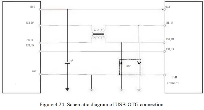 4.9.2. USB PCB Layout
The module supports high-speed USB interface with a rate of 480Mbps. Users are recommended to add a common mode inductor in the schematic design stage, which can effectively suppress EMI interference. If users need to increase electrostatic protection, please choose a TVS tube with parasitic capacitance less than 1pF.
Please refer to the following precautions when Layout:
- The common mode inductor should be close to the side of the USB connector .
- It is required to control 90 ohm differential impedance with an error of ±10%.
- The length error of the USB2.0 differential line is controlled within 2 mm.
- USB3.1 differential line is controlled within 0.7mm .
- If the USB has a charging function, please note that the VBUS trace should be as wide as possible.
- If there are test points, try to avoid bifurcation of the traces, and place the test points on the path of the traces.
Table 5.1 : Module internal USB trace length
| Pin | Signal | Length(mm) | Length Error (PN) |
| 146 | USB_HS_DP | 40.75 | 0.66mm |
| 145 | USB_HS_DM | 40.09 | |
| 186 | USB3_SS_TX0_P | 21.80 | 1 mm |
| 187 | USB3_SS_TX0_M | 22.80 | |
| 178 | USB3_SS_TX1_M | 25.98 | 1.1mm |
| 179 | USB3_SS_TX1_P | 27.08 | |
| 173 | USB3_SS_RX0_M | 27.43 | 0.5mm |
| 174 | USB3_SS_RX0_P | 26.93 | |
| 162 | USB3_SS_RX1_P | 25.41 | 0.18mm |
| 163 | USB3_SS_RX1_M | 25.23 |
4.10. Charging port
The QC3.0 charging scheme is integrated inside the SLM920 module. The charging-related content in this manual is only described with the internal charging scheme. The SM6125 platform uses the Qualcomm PMI632 internal integrated charging chip by default. This chip is in switching mode and has the characteristics of high efficiency. It integrates a 15-bit battery voltage detection ADC and a 15-bit current detection ADC . The maximum charging current can reach 3 A.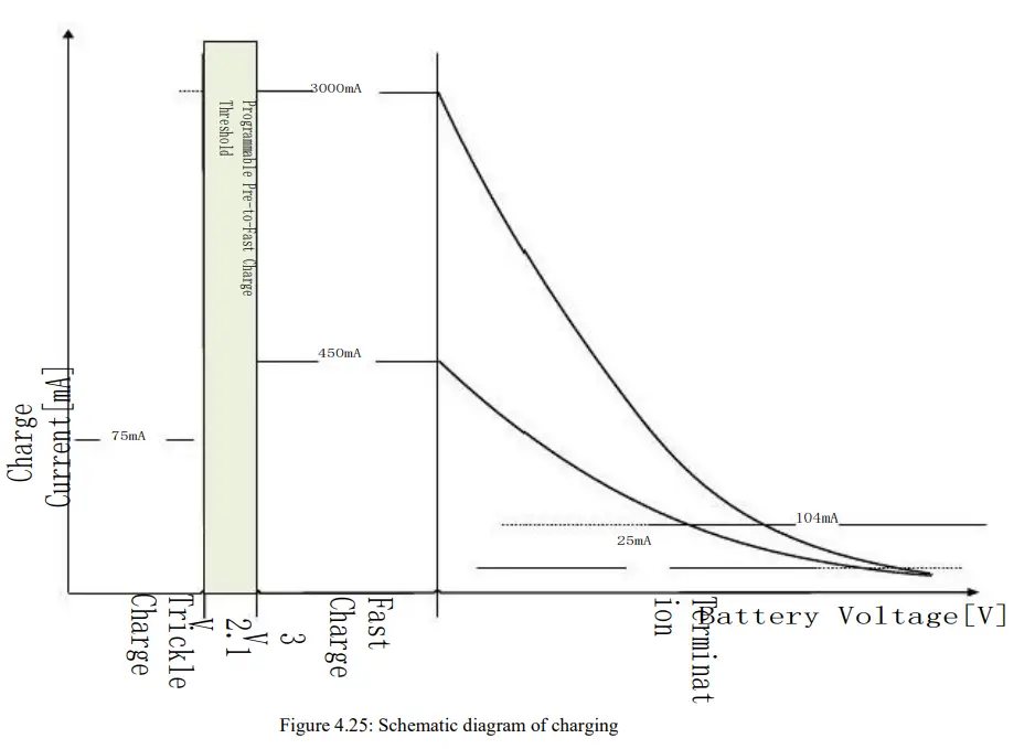 4.10.1. Charging detection
When the VBUS pin voltage is higher than 4.0V, a hardware interrupt will be generated inside the module, and the software will identify whether the charger is plugged in or the USB data cable is plugged in by judging the status of USB_HS_DP /USB_HS_DM .
4.10.2. Charge Control
SLM920 module can charge over-discharged batteries, and the charging process includes trickle charging, pre- charging, constant current, and constant voltage charging. When the battery voltage is lower than 2.1 V, the module is in a trickle charge state ; when the battery voltage is higher than 2.1V and lower than 3V , the module is in a precharge state; when the battery voltage is between 3V and 4.2 V, the The optimized constant current and constant voltage charging method for lithium batteries. The cut-off voltage , cut-off current , and back-charge voltage can be set according to the specific specifications of the battery and the charging time requirements.
4.10.3. BAT_THERM
SLM920 module has a battery temperature detection function, which can be realized by the user through BAT_THERM ( 149PIN ). This requires a thermistor (negative temperature coefficient) with a normal temperature of 10KΩ to be integrated inside the battery, and the thermistor is connected to the BAT_THERM pin. During the charging process, the software will read the voltage of the BAT_THERM pin to determine whether the battery temperature is too high. If the temperature is found to be too high or too low, it will stop charging immediately to prevent battery damage.
The battery charging connection diagram is shown in the following figure:  4.11. (U)SIM card interface
SLM920 can support two (U)SIM card interfaces at the same time to realize dual SIM dual standby. Support (U)SIM card hot swap, can automatically identify 1.8V and 3.0V cards. The following figure is the recommended interface circuit of (U)SIM. In order to protect the (U)SIM card, it is recommended to use a TVS device for electrostatic protection. (U) Devices of the peripheral circuit of the SIM card should be close to the SIM card holder.
The reference circuit is as follows:  4.11.1. SIM Card PCB Layout
The SIM card has a large area and has no anti-EMI interference devices, so it is more susceptible to interference. Therefore, when laying out, first ensure that the SIM card is far away from the antenna and the antenna extension cable inside the product, and is placed as close to the module as possible. When routing the PCB, pay attention to To protect the SIM_CLK signal, the SIM_DATA, SIM_RST and SIM_VDD signals of the SIM card should be kept away from the power supply and high-speed signal lines. If it is not handled properly, it will easily cause the card not to recognize or drop the card, so please follow the following principles when designing:
- In the PCB layout stage, the SIM card holder must be kept away from the GSM antenna;
- The SIM card wiring should be as far away as possible from RF lines, VBAT and high-speed signal lines, and the SIM card wiring should not be too long;
- The GND of the SIM card holder should maintain good connectivity with the GND of the module, so that the two GNDs are equipotential;
- In order to prevent SIM_CLK from interfering with other signals, it is recommended to protect SIM_CLK;
- It is recommended to place a 100nF capacitor on the SIM_VDD signal line close to the SIM card holder;
- Place TVS near the SIM card holder, the parasitic capacitance of the TVS should not be greater than 50pF, and a 51Ω resistor in series with the module can enhance ESD protection;
- The return path of VBAT has a large current passing through, so the SIM card wiring should avoid the return path of VBAT as much as possible.
4.12. SD card interface
SLM920 supports SD card interface , up to 256GB
The reference circuit is as follows: 4.13. I2C bus interface
The SLM920 module supports 6 sets of hardware I2C bus interface and two sets of camera dedicated CCI interface. The pin definitions and default functions are as follows:
Table 4.11: I2C interface pin description
| Name | Pin | Default function |
| CCI_I2C_SDA0 | 105 | For Camera |
| CCI_I2C_SCL0 | 104 | |
| GPIO28_SENSOR_I2C_SDA | 17 | Default for sensor |
| GPIO29_SENSOR_I2C_SCL | 18 | |
| GPIO4_APPS_I2C_SDA | 13 | Generic I2C |
| GPIO5_APPS_I2C_SCL | 14 | |
| GPIO14_I2C_SDA | 164 | Generic I2C |
| GPIO15_I2C_SCL | 165 | |
| CCI_I2C_SDA1 | 96 | For Camera |
| CCI_I2C_SCL1 | 95 | |
| GPIO6_TS_I2C_SDA | 234 | Generic I2C, default for TP |
| GPIO7_TS_I2C_SCL | 233 | |
| GPIO22_I3C_SDA | 184 | Generic I3C signal , default for sensor |
| GPIO23_I3C_SCL | 185 | |
| GPIO0_I2C_SDA | 254 | Generic I2C |
| GPIO1_I2C_SCL | 2 53 |
Note: When using as an I2C bus interface, connect a 2.2KΩ pull-up resistor to 1.8V.
4.14. Analog to Digital Converter (ADC)
The SLM920 module is provided by the power management chip with two ADC input ports PM6125_GPIO3_ADC ( 209 ) , PMI632_GPIO6 _WLED_PWM (4), and its performance parameters are as follows:
Table 4.12 : ADC performance parameters
| Describe | Minimum | Typical value | Maximum value | Unit |
| Input voltage range | 0 | 1.875 | V | |
| Analog input bandwidth | – | 500 | – | kHz |
| Sampling frequency | – | 4.8 | – | MHz |
4.15. PWM
The PM6125_GPIO8_PWM (112 PIN) pin can be used for LCD backlight adjustment, and the backlight brightness can be adjusted by adjusting the duty cycle.
4.16. MOTOR
SLM920 supports the motor function, which can be realized by the user through GND (8PIN) and VIB_DRV_LDO_P (9PIN) . Refer to the schematic diagram below , note that uF capacitors cannot be placed on the signal line. 4.17. Antenna Interface
The module provides MAIN antenna, DRX antenna, GPS antenna and five antenna interfaces for WiFi/BT_5G , WiFi/BT_2.4G antenna . In order to ensure that the user’s product has good wireless performance, the antenna selected by the user should meet the requirements of an input impedance of 50 ohms and a standing wave coefficient of less than 2 in the working frequency band.
4.17.1. MAIN Antenna
The module provides the MAIN antenna interface pin, Pin1 RF_MAIN. The antenna on the user’s motherboard should be connected to the antenna pin of the module using a microstrip line or stripline with a characteristic impedance of 50 ohms.
In order to facilitate antenna debugging and certification testing, an RF connector and antenna matching network should be added. The recommended circuit diagram is as follows: 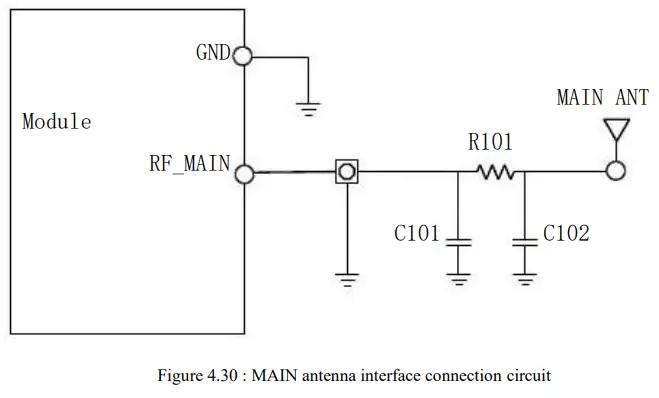 In the figure, R101, C101, and C102 are antenna matching devices, and the specific component values can be determined after the antenna factory has debugged the antenna. Among them, R101 defaults to 0R, and C101 and C102 default to not.
If there are fewer components that can be placed between the antenna and the module output, or when the RF test head is not required in the design, the antenna matching circuit can be simplified as shown in the following figure: 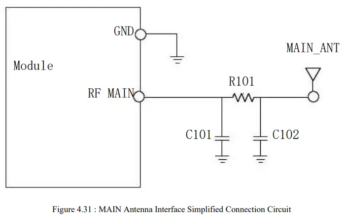 In the above picture, R101 is pasted 0R by default, and C101 and C102 are not pasted by default.
4.17.2 . DRX Antenna
The module provides the DRX antenna interface pin RF_DIV. The antenna on the user’s motherboard should be connected to the antenna pin of the module using a microstrip line or stripline with a characteristic impedance of 50 ohms.
In order to facilitate antenna debugging and certification testing, an RF connector and antenna matching network should be added. The recommended circuit diagram is as follows: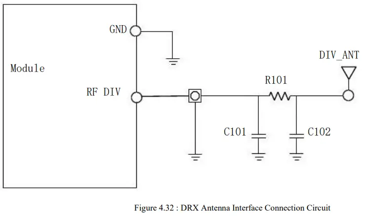 In the figure, R101, C101, and C102 are antenna matching devices, and the specific component values can be determined after the antenna factory has debugged the antenna. Among them, R101 defaults to 0R, and C101 andC102 default to not.
If there are fewer components that can be placed between the antenna and the module output, or when the RF test head is not required in the design, the antenna matching circuit can be simplified as shown in the following figure: 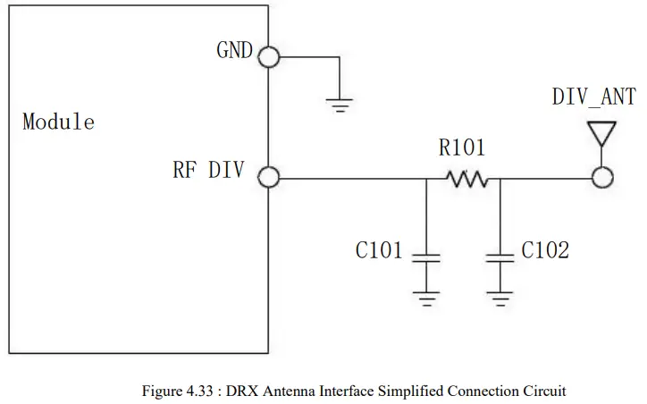 In the above picture, R101 is pasted 0R by default, and C101 and C102 are not pasted by default.
4.17.3. GPS Antenna
The module provides the GNSS antenna pin RF_GPS, the antenna on the user’s motherboard should use a microstrip line or stripline with a characteristic impedance of 50 ohms to connect to the antenna pin of the module. The LNA is integrated inside the module .
To improve GNSS reception performance, customers can use an external active antenna. The recommended circuit connection is shown in the following figure: 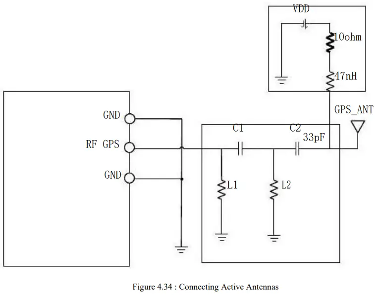 4.17.4. WiFi/BT Antenna
The module provides the WiFi/BT antenna pin RF_WIFI/BT, the antenna on the user’s motherboard should be connected to the module’s antenna pin using a microstrip line or stripline with a characteristic impedance of 50 ohms.
In order to facilitate antenna debugging and certification testing, an RF connector and antenna matching network should be added. The recommended circuit diagram is as follows: 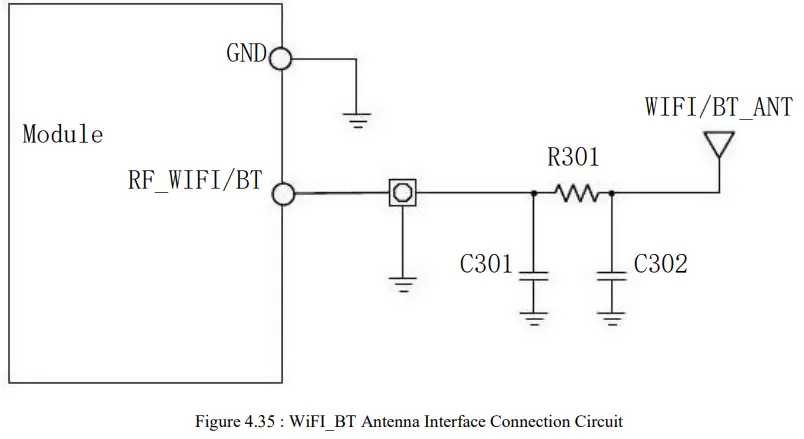 In the figure, R301, C301, and C302 are antenna matching devices, and the specific component values can only be determined after the antenna factory has debugged the antenna. Among them, R301 defaults to 0R, C301
If there are fewer components that can be placed between the antenna and the module output, or when the RF test head is not required in the design, the antenna matching circuit can be simplified as shown in the following figure: 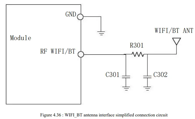 Note:
Note:
In the above picture, R301 is pasted 0R by default, and C301 and C302 are not pasted by default.
4.17.5. Antenna PCB Layout
Antenna part design, SLM920 module has a total of 5 antenna interfaces , they are : RF_MAIN , RF_D IV , GPS_ANT , WIFI_5G_ANT , WIFI_2.4G_ANT . Attention should be paid to the placement of components and RF wiring:
- The RF test head is used to test the conducted RF performance and should be placed as close as possible to the antenna pins of the module;
- The antenna matching circuit needs to be placed close to the antenna end;
- The connection from the antenna pin of the module to the antenna matching circuit must be controlled by 50 ohm impedance;
- The components and connections between the antenna pins of the module and the antenna connector must be kept away from high-speed signal lines and strong interference sources, and avoid crossing or paralleling with any signal lines on adjacent layers.
- The length of the radio frequency line between the antenna pin of the module and the antenna connector should be as short as possible, and the situation of crossing the entire PCB board should be absolutely avoided.
- If the antenna is connected by a coaxial radio frequency line, care should be taken to avoid making the coaxial radio frequency line straddle the SIM card, power supply circuit, and high-speed digital circuit to minimize mutual influence.
Electrical, reliability
5.1. Absolute Maximum
The table below shows the absolute maximum values that the module can withstand, exceeding these limits may result in permanent damage to the module.
Table 5.1 : Absolute Maximum Values
| Parameter | Minimum | Typical value | Maximum value | Unit |
| VBAT | -0.3 | – | 6 | V |
| VBUS | -0.3 | – | 16 | V |
| Peak current | – | – | 3 | A |
5.2. Operating temperature
The following table shows the operating temperature range of the module:
Table 5.2 : Module Operating Temperature
| Parameter | Minimum | Typical value | Maximum value | Unit |
| Operating temperature | -25 | – | 75 | °C |
| Storage temperature | -40 | – | 90 | °C |
5.3. Working voltage
Table 5.3 : Module Operating Voltage
| Parameter | Minimum | Typical value | Maximum value | Unit |
| VBAT | 3.5 | 4.2 | V | |
| VBUS | 3.6 | 5 | 10 | V |
| Hardware shutdown voltage | 3.4 | – | V |
5.4 . Digital Interface Features
Table 5.4 : Digital Interface Characteristics (1.8V)
| Parameter | Describe | Minimum | Typical value | Maximum value | Unit |
| Vih | Input high level voltage | 1.17 | – | 2.1 | V |
| VIL _ | Input low level voltage | -0.3 | – | 0.63 | V |
| VOH _ | Output high level voltage | 1.35 | – | 1.8 | V |
| VOL _ | Output low level voltage | 0 | – | 0.45 | V |
5.5. SIM_VDD Characteristics
Table 5.5 : SIM_VDD Characteristics
| Parameter | Describe | Minimum | Typical value | Maximum value | Unit |
| Vo | The output voltage | – | 2.95 | – | V |
| – | 1.8 | – | |||
| IO | Output current | – | – | 100 | mA |
5.6. PWRKEY Features
Table 5.6 : PWRKEY characteristics
| Parameter | Describe | Minimum | Typical value | Maximum value | Unit |
| PWRKEY | High level | 1.4 | 1.8 | – | V |
| Low level | – | 0 | 0.6 | V | |
| Effective time | 3000 | ms |
5.7. VCOIN Characteristics
Table 5.7 : VCOIN Characteristics
5.8. Static electricity protection
The modules are not specifically protected against electrostatic discharge. Therefore, users must pay attention to electrostatic protection when producing, assembling and operating the module.
5.9. Main RF performance of GNSS
The following table lists the main RF performance under GNSS conduction.
Table 5.15: Main RF performance parameters under GNSS conduction
| GNSS working frequency band: 1575.42MHZ | ||||
| GNSS carrier-to-noise ratio CN0: 39dB/Hz | ||||
| GNSS Sensitivity: | Capture (coldstart) | Capture (warmrestart) | Track | |
| -148 | -156 | -160 | dBm | |
| GNSS start time | Hot start | Wen Qi | Cold start | |
| TBD | TBD | TBD |
Important Notice to OEM integrators
- This module is limited to OEM installation ONLY.
- This module is limited to installation in mobile or fixed applications, according to Part 2.1091(b).
- The separate approval is required for all other operating configurations, including portable configurations with respect to Part 2.1093 and different antenna configurations
- For FCC Part 15.31 (h) and (k): The host manufacturer is responsible for additional testing to verify compliance as a composite system. When testing the host device for compliance with Part15 Subpart B, the host manufacturer is required to show compliance with Part 15 Subpart B while the transmitter module(s) are installed and operating. The modules should be transmitting and the evaluation should confirm that the module’s intentional emissions are compliant (i.e. fundamental and out of band emissions). The host manufacturer must verify that there are no additional unintentiona l emissions other than what is permitted in Part 15 Subpart B or emissions are complaint with the transmitter(s) rule(s).
The Grantee will provide guidance to the host manufacturer for Part 15 B requirements if needed.
Important Note
notice that any deviation(s) from the defined parameters of the antenna trace, as described by the instructions, require that the host product manufacturer must notify to XXXX that they wish to change the antenna trace design. In this case, a Class II permissive change application is required to be filed by the USI, or the host manufacturer can take responsibility through the change in FCC ID (new application) procedure followed by a Class II permissive change application.
End Product Labeling
When the module is installed in the host device, the FCC ID label must be visible through a window on the final device or it must be visible when an access panel, door or cover is easily re-moved. If not, a second label must be placed on the outside of the final device that contains the following text: “Contains FCC ID: 2APJ4-SLM920” The FCC ID can be used only when all FCC compliance requirements are met.
Antenna Installation
- The antenna must be installed such that 20 cm is maintained between the antenna and users,
- The transmitter module may not be co-located with any other transmitter or antenna.
- Only antennas of the same type and with equal or less gains as shown below may be used with this module. Other types of antennas and/or higher gain antennas may require additional authorization for operation.
| Antenna type | Band | Gain(dBi)) |
|
Glue Stick Antenna | 2400~2483.5MHz | 0.95 |
| 5150~5250MHz | 1.06 | |
| 5250~5350MHz | 0.88 | |
| 5470~5725MHz | 1.09 | |
| 5725~5850MHz | 1.07 | |
| GSM 850 | 2.81 | |
| PCS 1900 | 2.04 | |
| WCDMA B2 | 2.04 | |
| WCDMA B4 | 2.92 | |
| WCDMA B5 | 2.81 | |
| LTE B2 | 2.04 | |
| LTE B4 | 2.92 | |
| LTE B5 | 2.81 | |
| LTE B7 | 2.16 | |
| LTE B12 | 2.59 | |
| LTE B13 | 3.60 | |
| LTE B14 | 3.58 | |
| LTE B17 | 2.59 | |
| LTE B25 | 2.04 | |
| LTE B26 | 3.08 | |
| LTE B41 | 3.36 | |
| LTE B66 | 2.92 |
In the event that these conditions cannot be met (for example certain laptop configurations or co-location with another transmitter), then the FCC authorization is no longer considered valid and the FCC ID ID cannot be used on the final product. In these circumstances, the OEM integrator will be responsible for re-evaluating the end product (including the transmitter) and obtaining a separate FCC authorization.
Manual Information to the End User
The OEM integrator has to be aware not to provide information to the end user regarding how to install or remove this RF module in the user’s manual of the end product which integrates this module. The end user manual shall include all required regulatory information/warning as show in this manual.
Federal Communication Commission Interference Statement
This device complies with Part 15 of the FCC Rules. Operation is subject to the following twoconditions:
(1) This device may not cause harmful interference, and (2) this device must accept any interference received, including interference that may cause undesired operation. This equipment has been tested and found to comply with the limits for a Class B digital device, pursuant to Part 15 of the FCC Rules. These limits are designed to provide reasonable protection against harmful interference in a residential installation. This equipment generates, uses and can radiate radio frequency energy and, if not installed and used in accordance with the instructions, may cause harmful interference to radio communications. However, there is no guarantee that interference will not occur in a particular installation. If this equipment does cause harmful interference to radio or television reception, which can be determined by turning the equipment off and on, the user is encouraged to try to correct the interference by one of the following measures:
– Reorient or relocate the receiving antenna.
– Increase the separation between the equipment and receiver.
– Connect the equipment into an outlet on a circuit different from that to which the receiver is connected.
– Consult the dealer or an experienced radio/TV technician for help.
Any changes or modifications not expressly approved by the party responsible for compliance could void the user’s authority to operate this equipment. This transmitter must not be co-located or operating in conjunction with any other antenna or transmitter.
List of applicable FCC rules
This module has been tested and found to comply with part 22, part 24, part 27, part 90, 15.247 and 15.407 requirements for Modular Approval.
The modular transmitter is only FCC authorized for the specific rule parts (i.e., FCC transmitterrules) listed on the grant, and that the host product manufacturer is responsible for compliance toany other FCC rules that apply to the host not covered by the modular transmitter grant ofcertification.
If the grantee markets their product as being Part 15 Subpart B compliant (when it also contains unintentional-radiator digital circuity), then the grantee shall provide a notice stating that the final host product still requires Part 15 Subpart B compliance testing with the modular transmitter installed.
This device is intended only for OEM integrators under the following conditions:
(For module device use)
- The antenna must be installed such that 20 cm is maintained between the antenna and users, and
- The transmitter module may not be co-located with any other transmitter or antenna.
As long as 2 conditions above are met, further transmitter test will not be required. However, the OEM integrator is still responsible for testing their end-product for any additional compliance requirements required with this module installed.
Radiation Exposure Statement
This equipment complies with FCC radiation exposure limits set forth for an uncontrolled environment.
This equipment should be installed and operated with minimum distance 20 cm between the radiator & your body.
Production
6.1. Top and bottom views of the module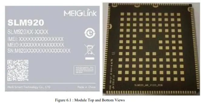 6.2. Recommended soldering furnace temperature curve
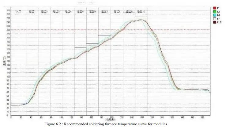 6.3. Moisture Sensitive Characteristics (MSL)
The SLM920 module complies with humidity class 3. Under the environmental conditions of temperature <30 degrees and relative humidity <60%, dry packaging executes J-STD-020C specification according to IPC/JEDEC standard. Shelf life is at least 6 months in the unopened condition under ambient conditions of temperature <40 degrees and relative humidity <90%. After unpacking, Table 22 lists the shelf life time of the modules corresponding to different moisture sensitivity grades.
Table 6.1 : Classification of humidity sensitivity levels
| Grade | Factory environment≦+30 ℃/60%RH |
| 1 | Indefinite warranty under ambient≦+30 ℃/85% RH |
| 2 | 1 year |
| 2a | 4 weeks |
| 3 | 168 hours |
| 4 | 72 hours |
| 5 | 48 hours |
| 5a | 24 hours |
| 6 | Use after forced baking. After baking, the modules must be patched within the time limit stated on the label. |
After unpacking, under the environmental conditions of temperature <30 degrees and relative humidity <60%, SMT patching should be carried out within 168 hours. If the above conditions are not met, baking is required. Note: Oxidation Risk: Baking SMD packages can cause metal oxidation and, if excessive, can lead to solderability issues during board assembly. The temperature and time to bake SMD packages, therefore limit solderability considerations. The cumulative bake time, at temperatures above 90°C and up to 125°C, should not exceed 96 hours.
6.4 Baking Requirements
Due to the moisture-sensitive nature of the module, the SLM920 should be fully baked before reflow soldering, otherwise the module may be permanently damaged during the reflow soldering process. The SLM 920 should be baked for 192 hours in a low temperature container at a temperature of 40°C+5°C/-0°C and a relative humidity of less than 5%, or the module should be baked in a high temperature container at 80°C±5°C 72 hours of baking. The user should note that the tray is not resistant to high temperature, the user should take the module out of the tray for baking, otherwise the tray may be damaged by high temperature.
Table 6.2 : Baking Requirements :
| Baking temperature | Humidity | Bake time |
| 40°C±5°C | <5% | 192 hours |
| 120°C±5°C | <5% | 4 hours |
Appendix
7.1. Related Documentation
Table 7.1 : Related Documentation
| Serial number | File name | Notes |
| [1] | GSM 07.07: | Digital cellular telecommunications (Phase 2+); AT command set for GSM Mobile Equipment (ME) |
| [2] | GSM 07.10: | Support GSM 07.10 multiplexing protocol |
| [3] | GSM 07.05: | Digital cellular telecommunications(Phase 2+); Use of Data Terminal Equipment–Data Circuit terminating Equipment(DTE–DCE) interface for Short Message service(SMS)and Cell Broadcast Service(CBS) |
| [4] | GSM 11.14: | Digital cellular telecommunications system (Phase 2+); Specification of the SIM Application Toolkit for the Subscriber Identity Module–Mobile Equipment (SIM–ME) interface |
| [5] | GSM 11.11: | Digital cellular telecommunications system (Phase 2+); Specification of the Subscriber Identity Module – Mobile Equipment (SIM–ME) interface |
| [6] | GSM 03.38: | Digital cellular telecommunications system (Phase 2+); Alphabets and language-specific information |
| [7] | GSM 11.10 | Digital cellular telecommunications system (Phase 2); Mobile Station (MS) conformance specification; Part 1: Conformance specification |
| [8] | AN_Serial Port | AN_Serial Port |
7.2. Terminology and Interpretation
Table 7.2 : Terms and Explanations
| The term | Explain |
| ADC | Analog-to-Digital Converter |
| AMR | Adaptive Multi-Rate |
| CS | Coding Scheme |
| CSD | Circuit Switched Data |
| CTS | Clear to Send |
| DTE | Data Terminal Equipment (typically computer, terminal, printer) |
| DTR | Data Terminal Ready |
| DTX | Discontinuous Transmission |
| EFR | Enhanced Full Rate |
| EGSM | Enhanced GSM |
| ESD | Electrostatic Discharge |
| ETS | European Telecommunication Standard |
| FR | Full Rate |
| GPRS | General Packet Radio Service |
| GSM | Global Standard for Mobile Communications |
| HR | Half Rate |
| IMEI | International Mobile Equipment Identity |
| Li-ion | Lithium-Ion |
| MO | Mobile Originated |
| MS | Mobile Station (GSM engine), also referred to as TE |
| MT | Mobile Terminated |
| PAP | Password Authentication Protocol |
| PBCCH | Packet Broadcast Control Channel |
| PCB | Printed Circuit Board |
| PCL | Power Control Level |
| PCS | Personal Communication System, also referred to as GSM 1900 |
| PDU | Protocol Data Unit |
| PPP | Point-to-point protocol |
| RF | Radio Frequency |
| RMS | Root Mean Square (value) |
| RX | Receive Direction |
| SIM | Subscriber Identification Module |
| SMS | Short Message Service |
| TDD | Time Division Distortion |
| TE | Terminal Equipment, also referred to as DTE |
| TX | Transmit Direction |
| UART | Universal Asynchronous Receiver & Transmitter |
| URC | Unsolicited Result Code |
| USSD | Unstructured Supplementary Service Data |
| phone book abbr | explain |
| FD | SIM fix dialing phonebook |
| LD | SIM last dialing phonebook (list of numbers most recently dialed) |
| MC | Mobile Equipment list of unanswered MT calls (missed calls) |
| ON | SIM (or ME) own numbers (MSISDNs) list |
| RC | Mobile Equipment list of received calls |
| SM | SIM phonebook |
| NC | Not connect |
![]() Shenzhen Meige Intelligent Technology Co., Ltd. Shanghai Branch
Shenzhen Meige Intelligent Technology Co., Ltd. Shanghai Branch
Contact address: 5th Floor, Building G, No.
2337 Gudai Road (Weijing Center), Minhang District ,
Shanghai
Postcode: 200233
Tel : +862154278676
Fax : +862154278679
Website: www.meigchina.com
Documents / Resources
 | Smart Technology SLM920 Data Transmission Wireless Module [pdf] User Guide SLM920 Data Transmission Wireless Module, SLM920, Data Transmission Wireless Module, Transmission Wireless Module, Wireless Module |