LINEAR TECHNOLOGY LTM4644EY Quad 4A Output Step Down µModule Regulator
Product Information:
- Product Name: Demo Manual DC1900A
- Model: LTM4644EY Quad 4A Output Step-Down
Description:
The Demo Manual DC1900A is a circuit board designed to evaluate the performance of the LTM4644EY Quad 4A Output Step-Down module. It features a few input and output capacitors and offers output voltage tracking through the TRACK/SS pin for supply rail sequencing. The board also supports external clock synchronization through the CLKIN pin. The LTM4644 data sheet should be read in conjunction with this demo manual before working on or modifying the demo circuit.
Product Usage Instructions:
The following are the step-by-step instructions for using the Demo Manual DC1900A: 1. Quick Start Procedure: a. Place the jumpers (JP1-JP8) in the following positions: – JP1: RUN1 ON – JP2: RUN2 ON – JP3: RUN3 ON – JP4: RUN4 ON – JP8: MODE1 CCM – JP7: MODE2 CCM – JP6: MODE3 CCM – JP5: MODE4 CCM b. Before connecting any supplies,preset the input voltage supply between 4.5V to 14V and set the load currents to 0A. c. Connect the loads, input voltage supply,and meters as shown in Figure 1 of the user manual. 2. Load Adjustment: a. Power off the circuit. b. Adjust the load currents for each phase within the range of 0A to 4A. c. Observe the load regulation, efficiency, and other parameters. 3. Increased Light Load Efficiency: a. To observe increased light load efficiency,place a Mode pin jumper (JP5-JP8) in the DCM Mode position.
Note:
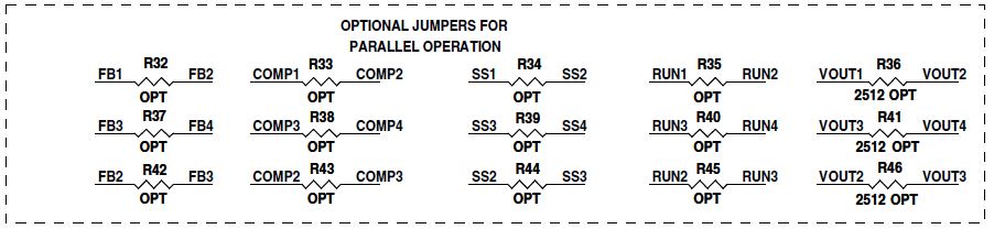
Optional jumper positions are available on the DC1900A to evaluate parallel operation of the LTM4644. For parallel operation of all 4 outputs, do not install any jumpers for R32-R46. Please refer to the user manual for additional information and circuit diagrams.
Parts List:
The following is the parts list for the required circuit components of the Demo Manual DC1900A: 1. C1, C3:
Capacitors 2. C6: Capacitor 3. C9, C17, C28, C36: Capacitors 4.
C10, C16, C29, C35: Capacitors 5. R3: Resistor 6. R4: Resistor 7.
R11: Resistors 8. R12: Resistor 9. U1: Integrated Circuit
Additionally, there are additional demo board circuit components listed in the user manual. For detailed circuit diagrams and further information, please refer to the user manual or visit the provided link for design files. Source: http://www.linear.com/demo/DC1900A
Description
Demonstration circuit 1900A features the LTM®4644EY μModule® regulator, a high-performance high-efficiency quad output step-down regulator. The LTM4644EY has an operating input voltage range of 4V to 14V and is able to provide up to 4A of output current from each of its phases.
Each output’s voltage is programmable from 0.6V to 5.5V.
The LTM4644EY is a DC/DC point of load regulator in a 9mm × 15mm × 5.01mm BGA package requiring only a few input and output capacitors. Output voltage tracking is available through the TRACK/SS pin for supply rail sequencing.
External clock synchronization is also available through the CLKIN pin. The LTM4644 data sheet must be read in conjunction with this demo manual prior to working on or modifying demo circuit 1900A.
Design files for this circuit board are available at http://www.linear.com/demo/DC1900A
Performance Summary
Specifications are at TA = 25°C
| PARAMETER | CONDITIONS | VALUE |
| Input Voltage Range | 4V to 14V | |
| Output Voltage VOUT | Jumper Selectable | VOUT1 = 3.3VDC, VOUT2 = 2.5VDC,
VOUT3 = 1.5VDC, VOUT4 = 1.2VDC |
| Maximum Continuous Load Current per Output | De-rating is necessary for certain operating conditions. See data sheet for details | 4ADC |
| Default Operating Frequency | 1MHz | |
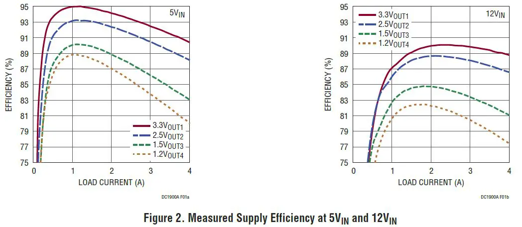
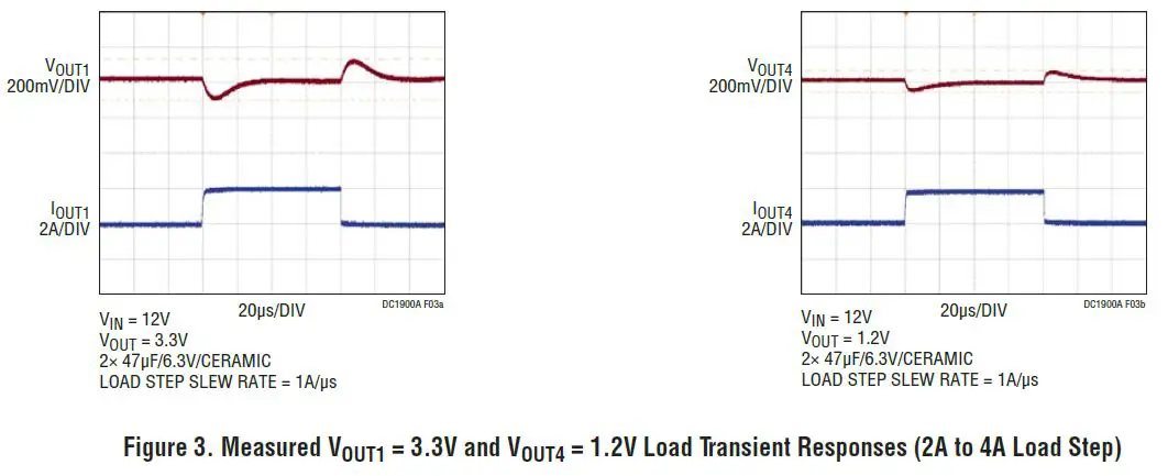
| Efficiency | VIN = 12V, VOUT1 = 3.3V, IOUT = 4A | 89% See Figure 2 |
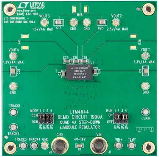
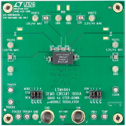
Board Photo
Quick Start Procedure
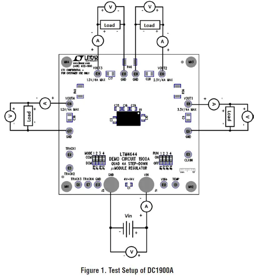
Demonstration circuit 1900A is an easy way to evaluate the performance of the LTM4644EY. Please refer to Figure 1 for test setup connections and follow the procedure below.
- With power off, place the jumpers in the following positions:
JP1 JP2 JP3 JP4 RUN1 RUN2 RUN3 RUN4 ON ON ON ON JP8 JP7 JP6 JP5 MODE1 MODE2 MODE3 MODE4 CCM CCM CCM CCM - Before connecting input supply, loads and meters, preset the input voltage supply to be between 4.5V to 14V. Preset the load currents to 0A.
- With power off, connect the loads, input voltage supply and meters as shown in Figure 1.
- Turn on input power supply. The output voltage meters for each phase should display the programmed output voltage within ± 2%.
- Once the proper output voltage is established, adjust the load currents for each phase within the 0A to 4A range and observe the load regulation, efficiency, and other parameters.
- To observe increased light load efficiency place a Mode pin jumper (JP5-JP8) in the DCM Mode position.
Note: Optional jumper positions are available on the DC1900A to allow for easy setup to evaluate parallel operation of the LTM4644. For example, to parallel all 4 outputs of the LTM4644 together stuff 0Ω jumpers for R32-R46.

Parts List
| ITEM | QTY | REFERENCE | PART DESCRIPTION | MANUFACTURER/PART NUMBER |
Required Circuit Components
| 1 | 2 | C1, C3 | CAP, 1206, CER. 22µF 25V X5R 20% | MURATA, GRM31CR61E226KE15L |
| 2 | 1 | C6 | CAP, 0603, X5R, 1uF, 16V 10% | AVX, 0603YD105KAT2A |
| 3 | 4 | C9, C17, C28, C36 | CAP, 1210 CER. 47µF 6.3V | AVX, 12106D476MAT2A |
| 4 | 4 | C10, C16, C29, C35 | CAP, 1206, X5R, 47uF, 6.3V, 20% | TAIYO YUDEN, JMK316BJ476ML |
| 5 | 1 | R3 | RES, 0603, 13.3kΩ 1% 1/10W | VISHAY CRCW060313K3FKEA |
| 6 | 1 | R4 | RES, 0603, 40.2kΩ 1% 1/10W | VISHAY CRCW060340K2FKEA |
| 7 | 2 | R11 | RES, 0603, 19.1kΩ 1% 1/10W | VISHAY CRCW060319K1FKEA |
| 8 | 1 | R12 | RES, 0603, 60.4kΩ 1% 1/10W | VISHAY CRCW060360K4FKEA |
| 9 | 1 | U1 | LTM4644EY, BGA-15X9-5.01 | LINEAR TECH.CORP. LTM4644EY |
Additional Demo Board Circuit Components
| 1 | 2 | C4, C5 | CAP, 1206, CER. 22µF 25V X5R 20% | MURATA, GRM31CR61E226KE15L |
| 2 | 1 | C2 | CAP, 7343, POSCAP 68µF 16V | SANYO, 16TQC68MYF |
| 3 | 6 | C7, C21, C22, C31, C41, C42 | CAP, 0603, OPTION | OPTION |
| 4 | 4 | C8, C18, C27, C37 | CAP, 7343, POSCAP, OPTION | OPTION |
| 5 | 8 | C11, C12, C14, C15, C30, C38, C33, C34 | CAP, 1206, CER., OPTION | OPTION |
| 6 | 2 | C13, C32 | CAP, 0603, CER., 100PF | AVX 06033C101KAT2A |
| 7 | 4 | R7, R8, R15, R16 | RES, 0603, 0Ω 1% 1/10W | VISHAY, CRCW06030000Z0ED |
| 8 | 1 | R28 | RES, 0805, 0Ω 5% 1/16W | VISHAY, CRCW08050000Z0EA |
| 9 | 4 | R19, R20, R21, R22 | RES, 0603, 150kΩ 5% 1/10W | VISHAY CRCW0603150KJNEA |
| 10 | 4 | R23, R24, R25, R26 | RES, 0603, 100kΩ 5% 1/10W | VISHAY CRCW0603100KJNEA |
| 11 | 4 | R9, R10, R17, R18 | RES, 0603, OPTION | OPTION |
| 12 | 12 | R32-R35, R37-R40, R42-R45 (OPT) | RES, 0603, OPTION | OPTION |
| 13 | 3 | R36, R41, R46 (OPT) | RES, 2512, 0Ω, OPTION | OPTION |
| 14 | 4 | C25, C26, C45, C46 | CAP, 0603, CER. 10µF 50V X7R | TDK, C1608X7R1H104M |
| 15 | 1 | R1 | RES., 0603, CHIP, 10k, 1% | VISHAY, CRCW060310K0FKED |
| 16 | 1 | R2 | RES, 0603, 1Ω 5% 1/10W | VISHAY,CRCW06031R00JNEA |
| 17 | 4 | R27, R29, R30, R31 | RES, 0603, 100kΩ 5% 1/10W | VISHAY CRCW0603100KJNEA |
Hardware
| 1 | 16 | E1, E3-E17 | TESTPOINT, TURRET 0.094″ | MILLMAX 2501-2-00-80-00-00-07-0 |
| 2 | 2 | J1, J2 | JACK, BANANA | KEYSTONE 575-4 |
| 3 | 8 | JP1-JP8 | JMP, 0.079 SINGLE ROW HEADER, 3 PIN | SULLINS, NRPN031PAEN-RC |
| 4 | 8 | XJP1-XJP8 | SHUNT, .079″ CENTER | SAMTEC, 2SN-BK-G |
| 5 | 4 | STAND-OFFS | STAND-OFF, SNAP ON, NYLON 0.375″ TALL | KEYSTONE, 8832(SNAP ON) |
Schematic Diagram


CUSTOMER NOTICE
LINEAR TECHNOLOGY HAS MADE A BEST EFFORT TO DESIGN A CIRCUIT THAT MEETS CUSTOMER-SUPPLIED SPECIFICATIONS; HOWEVER, IT REMAINS THE CUSTOMER’S RESPONSIBILITY TO VERIFY PROPER AND RELIABLE OPERATION IN THE ACTUAL APPLICATION. COMPONENT SUBSTITUTION AND PRINTED CIRCUIT BOARD LAYOUT MAY SIGNIFICANTLY AFFECT CIRCUIT PERFORMANCE OR RELIABILITY. CONTACT LINEAR TECHNOLOGY APPLICATIONS ENGINEERING FOR ASSISTANCE.
DEMONSTRATION BOARD IMPORTANT NOTICE
Linear Technology Corporation (LTC) provides the enclosed product(s) under the following AS IS conditions:
This demonstration board (DEMO BOARD) kit being sold or provided by Linear Technology is intended for use for ENGINEERING DEVELOPMENT OR EVALUATION PURPOSES ONLY and is not provided by LTC for commercial use. As such, the DEMO BOARD herein may not be complete in terms of required design-, marketing-, and/or manufacturing-related protective considerations, including but not limited to product safety measures typically found in finished commercial goods. As a prototype, this product does not fall within the scope of the European Union directive on electromagnetic compatibility and therefore may or may not meet the technical requirements of the directive, or other regulations.
If this evaluation kit does not meet the specifications recited in the DEMO BOARD manual the kit may be returned within 30 days from the date of delivery for a full refund. THE FOREGOING WARRANTY IS THE EXCLUSIVE WARRANTY MADE BY THE SELLER TO BUYER AND IS IN LIEU OF ALL OTHER WARRANTIES, EXPRESSED, IMPLIED, OR STATUTORY, INCLUDING ANY WARRANTY OF MERCHANTABILITY OR FITNESS FOR ANY PARTICULAR PURPOSE. EXCEPT TO THE EXTENT OF THIS INDEMNITY, NEITHER PARTY SHALL BE LIABLE TO THE OTHER FOR ANY INDIRECT, SPECIAL, INCIDENTAL, OR CONSEQUENTIAL DAMAGES.
The user assumes all responsibility and liability for proper and safe handling of the goods. Further, the user releases LTC from all claims arising from the handling or use of the goods. Due to the open construction of the product, it is the user’s responsibility to take any and all appropriate precautions with regard to electrostatic discharge. Also be aware that the products herein may not be regulatory compliant or agency certified (FCC, UL, CE, etc.).
No License is granted under any patent right or other intellectual property whatsoever. LTC assumes no liability for applications assistance,customer product design, software performance, or infringement of patents or any other intellectual property rights of any kind.
LTC currently services a variety of customers for products around the world, and therefore this transaction is not exclusive.
Please read the DEMO BOARD manual prior to handling the product. Persons handling this product must have electronics training and observe good laboratory practice standards. Common sense is encouraged.
This notice contains important safety information about temperatures and voltages. For further safety concerns, please contact a LTC application engineer.
Mailing Address:
Linear Technology
1630 McCarthy Blvd.
Milpitas, CA 95035
Copyright © 2004, Linear Technology Corporation
Linear Technology Corporation
1630 McCarthy Blvd., Milpitas, CA 95035-7417
408-432-1900 ● FAX: 408-434-0507 ● www.linear.com
Downloaded from Arrow.com.
Documents / Resources
 |
LINEAR TECHNOLOGY LTM4644EY Quad 4A Output Step Down µModule Regulator [pdf] User Guide LTM4644EY Quad 4A Output Step Down Module Regulator, LTM4644EY, Quad 4A Output Step Down Module Regulator, Step Down Module Regulator, Module Regulator, Regulator |