DELTA DVP02DA-E2 ES2-EX2 Series Analog Input Output Module

Thank you for choosing Delta’s DVP series PLC. DVP02DA-E2 (DVP04DA-E2) analog output module receives 2 (4) groups of 16-bit digital data from the PLC MPU and converts the digital data into 2 (4) points analog output signals (voltage or current). In addition, you can access the data in the module by applying FROM/TO instructions or write the output value of channels directly by using MOV instruction (Please refer to allocation of special registers D9900 ~ D9999).
- DVP02DA-E2 (DVP04DA-E2) is an OPEN-TYPE device. It should be installed in a control cabinet free of airborne dust, humidity, electric shock and vibration. To prevent non-maintenance staff from operating DVP02DA-E2 (DVP04DA-E2), or to prevent an accident from damaging DVP02DA-E2 (DVP04DA-E2), the control cabinet in which DVP02DA-E2 (DVP04DA-E2) is installed should be equipped with a safeguard. For example, the control cabinet in which DVP02DA-E2
(DVP04DA-E2) is installed can be unlocked with a special tool or key. - DO NOT connect AC power to any of I/O terminals, otherwise serious damage may occur. Please check all wiring again before DVP02DA-E2 (DVP04DA-E2) is powered up. After DVP02DA-E2 (DVP04DA-E2) is disconnected, Do NOT touch any terminals in a minute. Make sure that the ground terminal on DVP02DA-E2 (DVP04DA-E2) is correctly grounded in order to prevent electromagnetic interference.
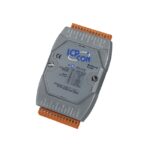
Product Profile & Dimension


External Wiring

Note 1: Please isolate analog output and other power wiring.
Note 2: If noise interferes from loaded input wiring terminal is significant, please connect a capacitor with 0.1 ~ 0.47μF 25V for noise filtering.
Note 3: Please connect power module terminal and analog output module terminal to system
I/O Terminal Layout

Electrical Specifications
| Digital/Analog module (02D/A & 04D/A) | |
| Power supply voltage | 24VDC (20.4VDC ~ 28.8VDC) (-15% ~ +20%) |
| Digital/Analog module (02D/A & 04D/A) | |
| Max. rated power consumption | 02DA: 1.5W, 04DA: 3W, supply by external power source. |
| Connector | European standard removable terminal block (Pin pitch: 5mm) |
| Protection | Voltage output is protected by short circuit. Short circuit lasting for too long may cause damage on internal circuits. Current output can be open circuit. |
| Operation/storage temperature | Operation: 0°C~55°C (temperature), 5~95% (humidity), Pollution degree2 Storage: -25°C~70°C (temperature), 5~95% (humidity) |
| Vibration/shock immunity | International standards: IEC61131-2, IEC 68-2-6 (TEST Fc)/ IEC61131-2 & IEC 68-2-27 (TEST Ea) |
| Series connection to DVP-PLC MPU | The modules are numbered from 0 to 7 automatically by their distance from MPU. Max. 8 modules are allowed to connect to MPU and will not occupy any digital I/O points. |
Functions Specifications
| Digital/Analog module | Voltage output | Current output | |
| Range of analog output | -10V ~ 10V | 0 ~ 20mA | 4mA ~ 20mA |
| Range of digital conversion | -32,000 ~ +32,000 | 0 ~ +32,000 | 0 ~ +32,000 |
| Max./Min. range of digital data | -32,768 ~ +32,767 | 0 ~ +32,767 | -6,400 ~ +32,767 |
| Hardware Resolution | 14 bits | 14 bits | 14 bits |
| Max. output current | 5mA | - | |
| Tolerance load impedance | 1KΩ ~ 2MΩ | 0 ~ 500Ω | |
| Analog output channel | 2 channels or 4 channels / each module | ||
| Output impedance | 0.5Ω or lower | ||
| Overall accuracy | ±0.5% when in full scale (25°C, 77°F) ±1% when in full scale within the range of 0 ~ 55°C (32 ~ 131°F) | ||
| Response time | 400μs / each channel | ||
| Digital data format | 2’s complement of 16 bits | ||
|
Isolation method | Optical coupler isolation between analog circuits and digital circuits. No isolation among analog channels. 500VDC between digital circuits and Ground 500VDC between analog circuits and Ground 500VDC between analog circuits and digital circuits 500VDC between 24VDC and Ground | ||
Control Register
| CR# | Attrib. | Register name | Explanation | |
| #0 | O | R | Model name | Set up by the system, model code: DVP02DA-E2 = H’0041; DVP04DA-E2 = H’0081 |
| #1 | O | R | Firmware version | Display the current firmware version in hex. |
| #2 | O | R/W | CH1 output mode setting | Output mode: Default = H’0000. Take CH1 for example: |
| CR# | Attrib. | Register name | Explanation | |
| #3 | O | R/W | CH2 output mode setting | Mode 0 (H’0000): Voltage output (±10V) Mode 1 (H’0001): Current output (0~+20mA) Mode 2 (H’0002): Current output (+4~+20mA) Mode -1 (H’FFFF): All channels are unavailable |
| #4 | O | R/W | CH3 output mode setting | |
| #5 | O | R/W | CH4 output mode setting | |
| #16 | X | R/W | CH1 output signal value | Voltage output range: K-32,000~K32,000. Current output range: K0~K32,000. Default: K0. CR#18~CR#19 of DVP02DA-E2 are reserved. |
| #17 | X | R/W | CH2 output signal value | |
| #18 | X | R/W | CH3 output signal value | |
| #19 | X | R/W | CH4 output signal value | |
| #28 | O | R/W | Adjusted Offset value of CH1 | Set the adjusted Offset value of CH1 ~ CH4. Default = K0 Definition of Offset: The corresponding voltage (current) input value when the digital output value = 0 |
| #29 | O | R/W | Adjusted Offset value of CH2 | |
| #30 | O | R/W | Adjusted Offset value of CH3 | |
| #31 | O | R/W | Adjusted Offset value of CH4 | |
| #34 | O | R/W | Adjusted Gain value of CH1 | Set the adjusted Gain value of CH1 ~ CH4. Default = K16,000. Definition of Gain: The corresponding voltage (current) input value when the digital output value = 16,000 |
| #35 | O | R/W | Adjusted Gain value of CH2 | |
| #36 | O | R/W | Adjusted Gain value of CH3 | |
| #37 | O | R/W | Adjusted Gain value of CH4 | |
| Adjusted Offset Value, Adjusted Gain Value: Note1: When using Mode 2, the channel do NOT provide setups for adjusted Offset or Gain value. Note2: When input mode changes, the adjusted Offset or Gain value automatically returns to defaults. | ||||
| #40 | O | R/W | Function: Set value changing prohibited | Prohibit set value changing in CH1 ~ CH4. Default= H’0000. |
| #41 | X | R/W | Function: Save all the set values | Save all the set values. Default =H’0000. |
| #43 | X | R | Error status | Register for storing all error status. Refer to table of error status for more information. |
| #100 | O | R/W | Function: Enable/Disable limit detection | Upper and lower bound detection, b0~b3 corresponds to CH1~CH4 (0: Disable/ 1: Enable). Default= H’0000. |
|
#101 |
X |
R/W |
Upper and lower bound status | Display the upper and lower bound status. (0: Not exceed /1: Exceeds upper or lower bound value), b0~b3 corresponds to Ch1~Ch4 for lower bound detection result; b8~b11 corresponds to CH1~CH4 for upper bound detection result.. |
| #102 | O | R/W | Set value of CH1 upper bound |
Set value of CH1~CH4 upper bound. Default = K32000. |
| #103 | O | R/W | Set value of CH2 upper bound | |
| #104 | O | R/W | Set value of CH3 upper bound | |
| #105 | O | R/W | Set value of CH4 upper bound | |
| #108 | O | R/W | Set value of CH1 lower bound |
Set value of CH1~CH4 lower bound. Default = K-32000. |
| #109 | O | R/W | Set value of CH2 lower bound | |
| #110 | O | R/W | Set value of CH3 lower bound | |
| #111 | O | R/W | Set value of CH4 lower bound | |
| #114 | O | R/W | Output update time of CH1 | Set value of CH1~CH4 lower bound. Setting |
| CR# | Attrib. | Register name | Explanation | |
| #115 | O | R/W | Output update time of CH2 | range:K0~K100. Default =H’0000. |
| #116 | O | R/W | Output update time of CH3 | |
| #117 | O | R/W | Output update time of CH4 | |
| #118 | O | R/W | LV output mode setting | Set the output mode of CH1~CH4 when the power is at LV (low voltage) condition. Default= H’0000. |
| Symbols: O: When CR#41 is set to H’5678, the set value of CR will be saved. X: set value will not be saved. R: able to read data by using FROM instruction. W: able to write data by using TO instruction. | ||||
| Description | |||||
| bit0 | K1 (H’1) | Power supply error | bit11 | K2048(H’0800) | Upper / lower bound setting error |
| bit1 | K2 (H’2) | Reserved | bit12 | K4096(H’1000) | Set value changing prohibited |
| bit2 | K4 (H’4) | Upper / lower bound error | bit13 | K8192(H’2000) | Communication breakdown on next module |
| bit9 | K512(H’0200) | Mode setting error | |||
| $Note: Each error status is determined by the corresponding bit (b0 ~ b13) and there may be more than 2 errors occurring at the same time. 0 = normal; 1 = error | |||||
Module Reset (available for firmware V1.12 or above): When modules need reset, write H’4352 to CR#0, then wait for one second and then power off and restart. The instruction initializes all parameter setups. To avoid the resetting process affecting the normal operation of other modules, it is recommended to connect only one module at a time.
Explanation on Special Registers D9900~D9999
When DVP-ES2 MPU is connected with modules, registers D9900~D9999 will be reserved for storing values from modules. You can apply MOV instruction to operate values in D9900~D9999.
When ES2 MPU is connected with DVP02DA-E2/DVP04DA-E2, the configuration of special registers is as below:
| Module #0 | Module #1 | Module #2 | Module #3 | Module #4 | Module #5 | Module #6 | Module #7 | Description |
| D1320 | D1321 | D1322 | D1323 | D1324 | D1325 | D1326 | D1327 | Model Code |
| D9900 | D9910 | D9920 | D9930 | D9940 | D9950 | D9960 | D9970 | CH1 output value |
| D9901 | D9911 | D9921 | D9931 | D9941 | D9951 | D9961 | D9971 | CH2 output value |
| D9902 | D9912 | D9922 | D9932 | D9942 | D9952 | D9962 | D9972 | CH3 output value |
| D9903 | D9913 | D9923 | D9933 | D9943 | D9953 | D9963 | D9973 | CH4 output value |
Adjust D/A Conversion Curve
Users can adjust the conversion curves according to the actual needs by changing the Offset value (CR#28 ~ CR#31) and Gain value (CR#34 ~ CR#37).
Gain: The corresponding voltage/current input value when the digital output value = 16,000.
Offset: The corresponding voltage/current input value when the digital output value = 0.
- Equation for voltage output Mode0: 0.3125mV = 20V/64,000

| Mode 0 (CR#2 ~ CR#5) | -10V ~ +10V,Gain = 5V (16,000),Offset = 0V (0) |
| Range of digital data | -32,000 ~ +32,000 |
| Max./Min. range of digital data | -32,768 ~ +32,767 |
- Current output – mode 1:

| Mode 1 (CR#2 ~ CR#5) | 0mA ~ +20mA,Gain = 10mA (16,000),Offset = 0mA (0) |
| Range of digital data | 0 ~ +32,000 |
| Max./Min. range of digital data | 0 ~ +32,767 |
Current output – mode 2:

| Mode 2 (CR#2 ~ CR#5) | 4mA ~ +20mA,Gain = 12mA (19,200),Offset = 4mA (6,400) |
| Range of digital data | 0 ~ +32,000 |
| Max./Min. range of digital data | -6400 ~ +32,767 |
Documents / Resources
 | DELTA DVP02DA-E2 ES2-EX2 Series Analog Input Output Module [pdf] Instruction Manual DVP02DA-E2 ES2-EX2 Series Analog Input Output Module, DVP02DA-E2, ES2-EX2 Series Analog Input Output Module, Analog Input Output Module, Input Output Module, Output Module, Module |