 InfiRay XcoreMicroIII Series Uncooled Thermal Imaging Module
 Product Overviews
Xcore MicroIII Series thermal imaging module is specially designed for applications that are sensitive to volume, weight, and power consumption. It is small in size, light in weight, and low in power consumption. It supports a variety of serial communication interfaces, video output interfaces, and lightweight infrared lenses. It is suitable for miniaturized handheld devices, enhanced night vision goggles (ENVG), UAVs, and multi-spectral systems, which supports a thorough thermal image solution. The temperature measuring products can be used in industrial measurement, power station measurement, security&surveillance measurement, machine vision etc.
Product Models
| supported) 07510X:75mm(T,T
H series is not supported) 10010X:100mm(T,TH series is not supported) |
Lens Parameters
| Module | MicroIII384/640 | |||||||
| Resolution | 384×288 | 640×512 | 384×288 | 640×512 | 384×288 | 640×512 | 384×288 | 640×512 |
| Focus | 4.1mm F1.2 | 5.8mm F1.2 | 9.1mm F1.0 | 13mm F1.2 | ||||
| Focus Type | Athermalization | Athermalization | Athermalization | Athermalization | ||||
| FOV | 59°×46° | 89°×75° | 44°×33° | 70°×57° | 28°×21° | 48°×38° | 20°×15° | 33°×26° |
| IFOV | 2.92mrad | 2.92mrad | 2.06mrad | 2.06mrad | 1.31mrad | 1.31mrad | 0.92mrad | 0.92mrad |
| Module | MicroIII384/640 | |||||||
| Resolution | 384×288 | 640×512 | 384×288 | 640×512 | 384×288 | 640×512 | 384×288 | 640×512 |
| Focus | 19mm F1.0 | 25mm F1.0 | 35mm F1.0 | 55mm F1.0 | ||||
| Focus Type | Athermalization | Athermalization | Athermalization | Athermalization | ||||
| FOV | 13°×10° | 22°×18° | 10°×7.9° | 17°×14° | 7.5°×5.6° | 12.5 ° × 10° | 4.8°×3.6° | 8°×6.4° |
| IFOV | 0.63mrad | 0.63mrad | 0.48mrad | 0.48mrad | 0.34mrad | 0.34mrad | 0.21mrad | 0.21mrad |
| Module | MicroIII384/640 | |||||||
| Resolution | 384×288 | 640×512 | 384×288 | 640×512 | ||||
| Focus | 75mm F1.0 | 100mm F1.0 | ||||||
| Focus Type | Thermalization | Thermalization | Thermalization | Thermalization | ||||
| FOX | 3.5°×2.6° | 5.9°×4.7° | 2.6°×2° | 4.4°×3.5° | ||||
| IFOV | 0.16mrad | 0.16mrad | 0.12mrad | 0.12mrad | ||||
Product Specification
| Module | MicroIII384/ MicroIII384S | MicroIII384T MicroIII384TH | MicroIII640/ MicroIII640S | MicroIII640T MicroIII640TH | |
| Detector Type | VOx Uncooled Infrared FPA | ||||
| Resolution | 384×288 | 640×512 | |||
| Pixel Pitch | 12μm | ||||
| Frame Rate | 50Hz /30Hz(1) | ||||
| Response Spectra | 8~14μm | ||||
| NETD | ≤50mK@25℃, F#1.0(≤40mK optional) | ||||
| TEC | No | ||||
| Image | |||||
| Brightness & Contrast Adjustment | Manual/Auto0/Auto1 | ||||
| Polarity | Black hot / white hot | ||||
| Palette | Support(2) | ||||
| Reticle | Display/disappear/move(2) | ||||
| Digital Zoom | 1.0~8.0×continuing zooming(step 0.1)(2) | ||||
|
Image Processing | Shutter-less(8) | ||||
| NUC | |||||
| Digital filtering/noise reduction | |||||
| DDE | |||||
| Image flip | Right-left/Up-down/Diagonal | ||||
| Power Supply | |||||
| Supply Voltage | 4~6VDC(3) | ||||
| Expansion boards support 3.5~18VDC(3) | |||||
| Typical Supply Voltage | 4VDC(3) | ||||
| Power Protection | Over-voltage/Under-voltage/Reverse Connection | ||||
|
Typical Consumption @25℃ | Excluding expansion board | <1.0W | <1.3W | ||
| Including expansion board | <1.2W | <1.6W | |||
| Interface | |||||
|
Video Output | Analog video | 1 channel PAL (4) Or 1 channel NTSC |
| Digital video | BT.656 | |
| 14Bit or 8Bit LVCMOS(5) | ||
| LVDS_H | ||
| Serial Communication Interface | RS-232 | |
| UART(3.3V) | ||
| Key | 4 keys | |
| Temperature Measurement Function(6) | ||
| Measuring Range | T series: -20℃~+150℃,0~+550℃ TH series: 0~60℃ | |
|
Measuring Accuracy | T series: ±3℃ or ±3% of reading(The larger value shall prevail)@ ambient temperature of -20℃~60℃ TH series: ±0.5℃@ target temperature 33℃~42℃;±1.0℃@ target temperature 20℃~33℃;±1.0℃@ target temperature 42℃~50℃ | |
| Measuring Tools | Spot, line, Area | |
| Physical Property | ||
| Weight (without lens and expansion board) | 21g±3g | |
| Size (without lens) | 26mm × 26mm | |
| Environmental adaptation | ||
| Operating Temperature | T series: -40℃~+80℃(Measuring temp. at -20℃~+60℃) TH series: -10℃~+50℃(16℃~32℃ for accurate temperature measurement) | |
| Storage Temperature | -45℃~+85℃ | |
| Humidity | 5~95%, non-condensing | |
| Vibration | 6.06g, Random vibration, all axial direction | |
| Shock | 80g, 4ms, Final peak sawtooth wave, 3 axial 6 direction | |
Table 2 Product Specification
Note:
- The detector frequency of PAL is 50Hz and 30Hz for NTSC.
- The digital video is without a palette, the reticle of displaying/disappearing/moving, digital zoom, and image flip function except BT.656.
- All these power supply voltage values represent the voltage on the module connector.
- PAL analog video output format is PAL-D.
- 14Bit or 8Bit LVCMOS digital video is only supported in the connector of Hirose 70 in the module.
- MicroIII384T and MicroIII640T supporting only.
- TH series requires the shell to meet the overall thermal conductivity of the shell heat flux≥800mW, Average heat of thermal conductors≥90J/℃.
- Only available for the S series.
User Interface Description
The Hirose 70PIN connector named DF40C-70DP-0.4V(51) is used on the imaging module of power supply interfaces, RS-232 interfaces, UART interfaces, analog video interfaces, BT.656 digital video interfaces, 14Bit or 8Bit LVCMOS digital video interfaces and 4 keys interfaces are contained on the connector. Users can adopt the Hirose 70Pin DF40HC(3.0)-70DS-0.4V(51) to implement the connection between imaging module and user expansion components.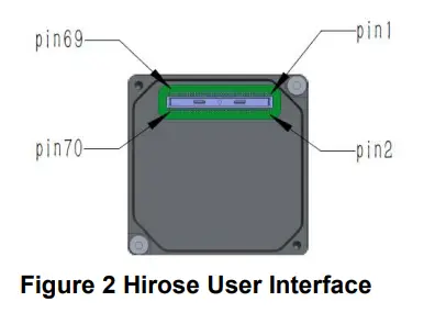
Hirose 70pin Connector Definition
| Pin NO. | Name | Type | Description | |||
| 1,2,3,4 | Power Supply | Power | Power Input(4~6VDC) (1) | |||
| 12,19~22, 42 | —— | —— | Not available | |||
| 15 | RS-232_RX | Input | RS-232 Serial communication interface (2) | |||
| 16 | RS-232_TX | Output | ||||
| 9,11 | VGND | Power | Ground of analog video (3) | |||
| 10 | VIDEO | Output | Analog video | |||
| 25 | DV1 | Data | BT.656 BT.1120 | Data | ||
| 26 | DV0 | Data LSB | Data | |||
| Pin NO. | Name | Type | Description | |||
| Output
Output | 16Bit or 14Bit or 8Bit LVCMOS Digital video(3.3V) | (3.3V) | LSB(BT.656) | |||
| 27 | DV3 | Data | Data | |||
| 28 | DV2 | Data | Data | |||
| 29 | DV5 | Data | Data | |||
| 30 | DV4 | Data | Data | |||
| 31 | DV7 | Data MSB(8bit) | Data MSB (BT.656) | |||
|
32 |
DV6 |
Data |
Data | |||
| 33 | DV9 |
16Bit or14Bit or 8Bit LVCMOS Digital video (3.3V) | Data | — | ||
| 34 | DV8 | Data | — | |||
| 35 | DV11 | Data | — | |||
| 36 | DV10 | Data | — | |||
| 37 | DV13 | Data MSB(14bit) | — | |||
| 38 | DV12 | Data | — | |||
| 24 | DV14 | Data | Data | |||
| 23 | DV15 | Data MSB(16bit) | Data MSB(BT.1120 ) | |||
| 39 | Line_Valid | Line valid signal | Line valid signal | |||
| 40 | Frame_Valid | Frame valid signal | Frame valid signal | |||
| 41 | Clock | Clock signal | Clock signal | |||
| 45 | UART_TX | Input/ Output | UART communication interface(3.3V)(2) | |||
| 46 | UART_RX | |||||
| 48 | KEY1 |
Input | Button interface (3.3V) | M(menu) | ||
| 50 | KEY2 | +(plus) | ||||
| 52 | KEY3 | -(minus) | ||||
| 54 | KEY4 | C(correction) | ||||
| Pin NO. | Name | Type | Description | |
| 47 | LVDS_CLK+ |
Output |
LVDS_H (VCCIO=2. 5V) | Clock signal |
| 49 | LVDS_CLK- | |||
| 51 | LVDS_DATA0+ | Data | ||
| 53 | LVDS_DATA0- | |||
| 57 | LVDS_DATA1+ | Data | ||
| 59 | LVDS_DATA1- | |||
| 61 | LVDS_DATA2+ | Data | ||
| 63 | LVDS_DATA2- | |||
| 65 | LVDS_DATA3+ | Data | ||
| 67 | LVDS_DATA3- | |||
| 58 | IO0 |
Input/ Output | Reserved | |
| 60 | IO1 | Reserved | ||
| 62 | IO2 | Reserved | ||
| 64 | IO3 | Reserved | ||
| 66 | IO4 | Reserved | ||
| 68 | IO5 | Reserved | ||
| 5,6,7,8, 13,14,17, 18,43,44, 55,56,69, 70 |
GND |
Power |
Ground of power supply (3) | |
Note:
- Typical value of power supply is 4VDC, setup time(10%~90%)<4mS, peak current<1.0A, ripple&noise<40mVp-p.
- The TX and RX in serial communication interface represent the transfer and receive of this module.
- GND and VGND are shorted internally.
Expansion Board List
| Model | Figure | IRay PN | Function | Connectors | Fit module |
 | l USB power supply, typical 5 | MicroIII384, | |||
| MRIII00V11 0F016C | 2030101240 | V DC l USB communication l USB UVC Video | TYPE C | MicroIII640, MicroIII640T, MicroIII384T | |
| l Power input3.5~18 | Hirose 20 pin DF52-20S- 0.8H connector Molex 20 pin 52745-2097 connector | |||
| VDC, typical 12 | |||||
| VDC | MicroIII384, | ||||
| MRIII00V10 0F012C | 2030100889 | l RS-232,Uart /RS- 422 l Analog video | MicroIII640, MicroIII640T, | ||
| l BT.656 digital | MicroIII384T | ||||
| video | |||||
| l 4 Keys | |||||
|
| l Power input: | ||||
| MRIII00V10 0F011C | 2030100902 | 3.5~18v, typical 12 VDC l RS232, RS422 l 4 keys l LVDS_H digital video l Analog video | DF56C-30S- 0.3V(51) | MicroIII384, MicroIII640, MicroIII640T, MicroIII384T | |
|
| l Power input: | ||||
| MRIII00V10 0F008C | 2030101595 | 3.5~18v, typical 12 VD l RS232,RS422 l 4 keys l Cameralink digital video l Analog video | DF56C 30S- 0.3V(51) | MicroIII384, MicroIII640, MicroIII640T, MicroIII384T |
![InfiRay-XcoreMicroIIL-Series-Uncooled-Thermal-Imaging-Module-5]](https://manuals.plus/wp-content/uploads/2022/08/InfiRay-XcoreMicroIIL-Series-Uncooled-Thermal-Imaging-Module-5.png)

| Model | Figure | IRay PN | Function | Connectors | Fit module |
| l Power input: | ||||
| MRIII00V11 0F017C | 2030101721 | 3.5~18v, typical 12 VDC l RS232 RS422 l 4 keys l MIPI digital video l Analog video | DF56C-30S- 0.3V(51) | MicroIII384, MicroIII640, MicroIII640T, MicroIII384T | |
| Please contact salesman to confirm model. |  | Specific model corresponde nce | l Used for fine-tuning of lens- focus | None | MicroIII 384, MicroIII 640, MicroIII 640T, MicroIII384T |
LVCOMS Digital Video
LVCMOS digital video includes 1 Clock signal (Clock), 1 Line_Valid signal and 1 valid frame signal(Frame_Valid), and 14 data signals (dv0-dv13).Pixel data bits are divided into 14 bit and 8 bit, when the user chooses to lose. When RAW data or temperature (TMP) data is selected, there is all together 14-bit data, namely DV[13:0], where DV0 is LSB and DV13 is the MSB. When the user selects the data after the output image processing (DRC), there is all together 8-bit data, namely DV[7:0], where DV0 is LSB and DV7 is the MSB. LVCMOS digital video can be turned on or off with control commands. While the LVCMOS digital video is turned on, you can choose to output raw data (ORG) or non-uniform correction (NUC) data, or image processing (DRC) data.
When DRC data is selected, the thermal camera module does not support the function of digital zoom and temperature information display.
| Product model | Clock frequency |
| M3384 | 12.857MHz |
| M3640 | 19.286MHz |
| M3 384T | 6.4286MHZ |
| M3 640T | 12.857MHZ |
 Note:
Note:
- Clock rising edge sampling is recommended for DV.
- Line_Valid and Frame_Valid are both high-level valid.
- after Line_Valid is valid, it lasts for n Clock, which corresponds to the data of the first column to the last column of the row in turn.
LVDS Digital Video
LVDS digital video includes 1 clock signal (LVDS_CLK) and 4 data signals (LVDS_DATA1, LVDS_DATA2, LVDS_DATA3, and LVDS_DATA4), which can be easily analyzed by domestic mainstream video coding & decoding chip.
LVDS digital video can be turned on or off with control commands. In the open state, choose to output raw data (ORG) or non-uniformity correction (NUC) data, or image processing (DRC) data.
When choosing to use image processing (DRC) data, the core component does not support the function of electronic zoom and temperature information display.
| Product model | Clock frequency (LVDS_CLK) |
| M3 384 | 22.500MHz |
| M3 640 | 33.750MHz |
| M3 384T | 11.250MHZ |
| M3 640T | 22.500MHZ |

| H0 | H1 | H2 | H3 | H4 | H5 | H6 | H7 | |
| BLANK LINE | 3FFF | 0000 | 0000 | 2AC0 | 3FFF | 0000 | 0000 | 2D80 |
| VALID LINE | 3FFF | 0000 | 0000 | 2000 | 3FFF | 0000 | 0000 | 2740 |
BT.1120 Digital Video
Bt.1120 digital video is the line-by-line output signal, including the Clock signal (Clock), frame effective signal, line effective signal, 16 data signals (dv0-dv15). FIG. 5 sequence diagram takes the n×m array as an example:
When choosing to use bt.1120 digital video, the thermal camera component does not support the electronic zoom, temperature information display function.
BT.656 Digital Video
Bt.656 digital video, including 1 Clock signal (Clock) and 8 data signals (DV0-DV7).
BT.656 digital video supports all functions of the thermal camera module (see table 1 for image adjustment and temperature measurement), including brightness/contrast adjustment, polarity selection, color Palette selection, reticle control, digital zoom and image flip functions, and only supports output image processing (DRC) data.
CDS_2 digital video (only available for T-series)
CDS_2 digital video contains 1 Clock signal (Clock), 1 frame valid signal (Vsync), 1 line valid signal (Hsync), and 16 DATA signals (DATA).The video data consists of two parts, the first half of each row of data is divided into an image, which conforms to the YUV422 format. The high 8 bits is the brightness component, the low 8 bits is the chroma component, and the image supports pseudo-color mapping. The second half of each row is divided into temperature data. The actual significant bit is 14 bits, and the higher two bits complement 0.
Remark:
- The output image data format is YUV, the high 8bit is Y, the low 8bit is UV.
- “T” stands for temperature data (effective data bits are 14 bits lower, two bits higher complement 0), “TH” stands for 8 bits higher, and “TL” stands for 8 bits lower.
- External synchronization signal mode is adopted. “Vsync” represents the frame synchronization signal and “Hsync” represents row synchronization signal.
- The output data of each row is 2 times of the array N, such as a thermal camera module with array of 640*512, each row contains 640*2=1280 clock cycles (N = 640), and each frame contains 512 rows (M=512).
Product Model CLK Frequency(Clock) M3 384T 22.5MHZ M3 640T 45.0MHZ Table 7 CDS_2 CLK Frequency
MIPI Protocol
MIPI digital video includes 1 pair of source-synchronized differential clocks (MIPI_CLK+,MIPI_CLK-), and 4 pairs of differential data lines (MIPI_DATA0+,MIPI_DATA0-,MIPI_DATA1+,MIPI_DATA1-,MIPI_DATA2+, MIPI_DATA2-, MIPI_DATA3+, MIPI_DATA3-).
The clock signal enters the high-speed mode at the beginning of each frame and exits it at the end of the frame. The inter-frame is in the low-power mode (the data and clock lines are both at a 1.2V high level). The data line sends a packet header at the beginning of each frame, and a packet footer at the end of the frame. There are 192 data packets between the packet header and the packet footer, and each long packet data contains one line of valid data. The data format and electrical characteristics comply with the CSI-2 standard and D-PHY protocols with an output clock frequency 200MHz and 4lane data lines.
Imaging Modules
After the module is connected to power, it will start to output MIPI digital video and data of 640*512 array. The data format can be set to RAW8, RAW14, and YVU422 through the refreshing program, and the settings are as follows:
| Data Format | Module Setting | Module Output |
| RAW8 | DRC+LVCOMS | DRC |
| RAW14 | NUC+LVCOMS | NUC |
| YVU422 | BT1120 | DRC with palette |
The data format is the standard MIPI CSI-2 protocol, as shown below.
- RAW8

- RAW14

- YUV422

Thermographic Module
After the module is connected to power, it will start to output MIPI digital video and data of 1280*512 array. The data format can be set to YVU422 format through the refresh program. The module settings are as follows:
| Data Format | Module Setting | Module Output |
| YUV422 | CDS2 | DRC with palette (left) +temperature(right) |
The output of YUV422 is 1280*512 array data. The first 640 pixels of line valid data are image data, which can be output directly in YVU422 format. The last 640 pixels of line valid data are temperature data, which requires that the UYVY backend of 2 pixels is spliced into two 16-bit temperature data by itself, with the more significant byte first. The data format of one line is shown in the figure below.
Dimension
Announcements
To protect you and others from injury or to protect your equipment from damage, please read all the following information before using your equipment.
- The product shall not face towards the sun or other high-intensity radiation sources directly;
- The optimal environment temperature for operating is – 20 ℃ to 50 ℃;
- The detector window shall not be touched or hit with hands or other objects;
- The equipment and cables shall not be touched with wet hands;
- Please do not bend or damage cables;
- Scrubbing your equipment with diluents is prohibited;
- Do not unplug and plug cables when the power is on;
- the Wrong cable should not be connected in case that brings damages to the equipment;
- Please pay attention to preventing static electricity;
- Please do not disassemble the equipment. If there is any fault, please contact us, and professional personnel will carry out maintenance.
Supports and Services
Technical Supports
- Modification design can be carried out according to different application requirements of users.
- System training can be carried out for users’ technical staff and operators.
After-sales Services
MicroIII is developed and manufactured by IRay. It has good after-sales service guarantees such as technical support and equipment maintenance. If you have any questions, please contact us.
Company Information
IRay Technology Co., Ltd.
Website: www.iraytek.com
Tel: 86-0535-3410623
Fax: 86-0535-3410610
E-mail: sales@iraytek.com, support@iraytek.com
Address: 11th Guiyang Street, YEDA Yantai 264006, P. R. China
©IRay Technology Co., Ltd. 2020.All right reserved worldwide. All contents in this manual, including words, pictures, images, etc., belong to IRAY TECHNOLOGY CO., LTD. (Hereinafter referred to as “THE COMPANY” or “IRAY TECHNOLOGY”). No part of the manual, in whole or in parts, may be copied, photocopied, translated, or transmitted without the prior written permission of IRAY TECHNOLOGY.
This manual is used as a guide. The photos, graphics, diagrams and illustrations provided in the manual are only used to explain, which may be different from the specific product. Please refer to the real object. We try our best to make sure the contents in this manual are accurate. We do not provide any representations or warranties in this manual.
If you need the latest version of this manual, please contact us. It is recommended that you use this manual with the guidance of professionals.
Revision History
| Version | Date | Comments | Remark | Revised by | Checked by |
| V0.1 | 2019-03 | Initial Version | |||
| V0.2 | 2019-03 | Add brightness/contract mode, digital zoom, products module, extension board. | |||
| V0.3 | 2019-04 | Add two product models without lens, expansion board. | |||
| V0.4 | 2019-09 | Modify lens code in product model table | Page 1 | ||
| V0.5 | 2019-12 | Add digital video description | |||
| V0.6 | 2020-02 | Add TH series | |||
| V0.7 | 2020-03 | Add TH house requirements | |||
| V0.8 | 2020-05 | 16bit LVCMOS description added | |||
| V0.9 | 2020-05 | flange with no lens dia. description added | Page 2 | ||
| V1.0.0 | 2020-06 | 5.8mm lens description revised | Page 2 | ||
|
V1.0.1 |
2020-06 | Modify the connector model on MRIII00V100F011C Add a description in temperature measurement range | Page 9
Page 5 | ||
| V1.0.2 | 2020-06 | Add two user expansion boards Revise the power supply range of expansion board | Ma Yanjing Lin Wenjuan | Lu Fengjuan | |
| V1.0.3 | 2020-09 | Revise pin definition of 51,53,23 and | Wu | Lu Fengjuan |
| 24. | Changhao Lin Wenjuan | ||||
|
V1.0.4 |
2020-10 | Add CLK frequency of MicroⅢ 384T and MicroⅢ 640T | Wu Changhao Lin Wenjuan | ||
| V1.0.5 | 2020-11 | Add CLK frequency of CDS_2 and remarks of shutterless | |||
| V1.0.6 | 2020-11 | Modify CLK frequency of CDS_2 | |||
| V1.0.7 | 2020-12 | Revise pin definition of 48,50,52 and 54 | |||
| V1.0.8 | 2021-3 | Add MIPI description | |||
| V1.0.9 | 2021-4 | Revise description of LVCMOS Add a note for lens parameters | |||
| V1.1.0 | 2021-4 | Revise F-number of 9.1mm lens | |||
| V1.1.1 | 2021-6 | Revise the FOV parameters in Table 1 |
Documents / Resources
 | InfiRay XcoreMicroIII Series Uncooled Thermal Imaging Module [pdf] User Manual XcoreMicroIII Series, Uncooled Thermal Imaging Module, Thermal Imaging Module, Imaging Module, XcoreMicroIII Series, Module |


