
1. Introduction
This manual provides essential information for the proper setup, operation, and maintenance of the SCFPGA PZ-FH9009 ADRV9009 FMC Module. The PZ-FH9009 is a high-performance Software Defined Radio (SDR) front-end designed for advanced wireless systems, integrating the Analog Devices ADRV9009 transceiver. It offers extensive capabilities for signal processing in various applications.
2. Product Overview and Features
The SCFPGA PZ-FH9009 FMC Module is engineered for demanding RF applications, providing a versatile platform for wireless research, radar prototyping, and industrial communication systems.

Figure 2.1: Top view of the SCFPGA PZ-FH9009 ADRV9009 FMC Module. This image displays the overall layout of the module, including the RF connectors and the FMC HPC connector.
Key Features:
- Wideband Frequency Coverage: Operates from 75MHz to 6GHz, supporting both Time Division Duplex (TDD) and Frequency Division Duplex (FDD) modes for flexible RF signal transmission and reception.
- High-Performance ADRV9009 Chipset: Incorporates the Analog Devices ADRV9009 transceiver, featuring a 16-bit Analog-to-Digital Converter (ADC) and a 14-bit Digital-to-Analog Converter (DAC) for superior signal fidelity and dynamic range.
- Flexible Clock Options: Supports both onboard and external clock sources via dedicated CLK IN/OUT ports, facilitating phase synchronization across multiple systems.
- Advanced JESD204B Interface: Utilizes a high-speed JESD204B digital interface for low-latency, high-throughput data communication with compatible FPGA carrier boards.
- FMC HPC Interface & Compact Size: Designed with a High-Pin-Count (HPC) FMC connector, ensuring compatibility with Xilinx FPGA platforms. The compact form factor measures 69mm × 76.5mm.
3. Components and Package Contents
The following items are typically included with your PZ-FH9009 FMC Module. Please verify all components upon receipt.

Figure 3.1: Contents of the PZ-FH9009 FMC Module package. This image shows the main ADRV9009 SDR Board along with a heat sink, glue stick antennas, and adaptor cables.
- ADRV9009 SDR Board (PZ-FH9009)
- Heat Sink
- Glue Stick Antenna (2.4/5.8G Dual Band) x 4
- Adaptor Cable x 6
Module Component Identification:

Figure 3.2: Key components and interfaces on the PZ-FH9009 module. This diagram highlights the TRX (Transmitter/Receiver) ports, RX (Receiver) ports, the ADRV9009 chip, External Clock Input/Output, Clock Chip, and the FMC HPC connector.

Figure 3.3: Location of the External Local Oscillation Input on the PZ-FH9009 module. This port allows for the connection of an external LO source for enhanced synchronization and performance.
4. Setup Instructions
Proper installation is crucial for the functionality and longevity of the PZ-FH9009 module. Follow these steps carefully:
- Prepare the Carrier Board: Ensure your FPGA carrier board is powered off and properly configured to accept an FMC HPC module. Refer to your carrier board's documentation for specific requirements.
- Install Heat Sink: Apply thermal paste (not included, if required) to the ADRV9009 chip and securely attach the provided heat sink. Ensure good contact for optimal thermal dissipation.
- Mount the FMC Module: Carefully align the PZ-FH9009 module with the FMC HPC connector on your carrier board. Apply even pressure to seat the module fully. Secure it with screws if your carrier board provides mounting points.
- Connect Antennas/RF Cables: Attach the provided glue stick antennas or appropriate RF cables to the TRX and RX ports. Ensure connections are finger-tight.
- Clock and LO Connections (Optional): If using external clocking or an external local oscillator, connect the respective cables to the CLK IN/OUT and External LO ports as needed.
- Power On: After all connections are secure, power on your FPGA carrier board.
5. Operating Instructions
Operating the PZ-FH9009 module typically involves interaction with the FPGA on the carrier board. This section provides general guidelines.
- FPGA Configuration: Load the appropriate FPGA bitstream onto your carrier board. This bitstream should include the necessary JESD204B interface logic and control for the ADRV9009 transceiver.
- Software Interface: Utilize the provided software development kit (SDK) or custom software to configure the ADRV9009 registers, set operating frequencies, bandwidths, gain, and other parameters.
- Data Acquisition and Transmission: Once configured, the module can begin receiving (RX) and transmitting (TX) RF signals. Data will be transferred to/from the FPGA via the JESD204B interface.
- Monitoring: Monitor the module's status, temperature, and signal integrity through your software interface.
Note: Specific operating procedures will depend on your FPGA design and software implementation. Refer to the Analog Devices ADRV9009 documentation and your FPGA development resources for detailed programming information.
6. Maintenance
The PZ-FH9009 module is designed for reliable operation with minimal maintenance. Adhere to the following guidelines:
- Keep Clean: Ensure the module and its connectors are free from dust and debris. Use a soft, dry brush or compressed air for cleaning. Avoid liquid cleaners.
- Environmental Conditions: Operate the module within its specified temperature and humidity ranges (refer to specifications). Avoid extreme temperatures or sudden changes.
- Secure Connections: Periodically check that all RF cables and the FMC connector are securely seated.
- Thermal Management: Ensure the heat sink remains properly attached and that airflow around the module is not obstructed to prevent overheating.
7. Troubleshooting
If you encounter issues with your PZ-FH9009 module, consider the following common troubleshooting steps:
- No Power/Module Not Detected:
- Verify the FPGA carrier board is powered on.
- Ensure the PZ-FH9009 module is correctly seated in the FMC HPC connector.
- Check for any visible damage to the module or carrier board.
- RF Signal Issues (No TX/RX):
- Confirm antennas or RF cables are properly connected to the correct ports (TRX/RX).
- Verify the FPGA bitstream is loaded and the ADRV9009 is correctly initialized and configured via software.
- Check frequency, gain, and bandwidth settings in your software.
- Ensure external clock or LO sources (if used) are active and correctly connected.
- Data Transfer Errors (JESD204B):
- Review your FPGA JESD204B IP core configuration and ensure it matches the ADRV9009 settings.
- Check for clocking issues between the module and the FPGA.
- Overheating:
- Ensure the heat sink is properly installed and making good contact with the chip.
- Verify adequate airflow around the module.
- Reduce power consumption or operating frequency if possible, as a temporary measure.
If problems persist, consult the SCFPGA support resources or the Analog Devices ADRV9009 documentation.
8. Specifications
Detailed technical specifications for the SCFPGA PZ-FH9009 ADRV9009 FMC Module:

Figure 8.1: Overview of the PZ-FH9009 FMC Module's key specifications. This table summarizes the module's capabilities and physical characteristics.
| Feature | Specification |
|---|---|
| FMC Module | ADRV9009 |
| Bits | 16bit ADC & 14bit DAC |
| Antenna Switch | Support Half-duplex and Full-duplex, TDD/FDD Mode |
| Coverage Frequency | 75MHz-6GHz |
| Bandwidths | Transmit up to 450MHz, Receive up to 200MHz |
| Power Amplifier | Broadband, High Power, Linear Amplification 22dbm |
| RF Impedance | Matching 50Ω |
| Digital Interface | JESD204B |
| Clock | On-board Clock or External Input Clock |
| FMC Interface | HPC |
| Form Factors | 2.72 inch x 3.01 inch (69mm x 76.5mm) |
| Product Dimensions | 3.01 x 2.72 x 0.1 inches; 7.05 ounces |
| Maximum Supply Voltage | 5 Volts |
| Upper Temperature Rating | 85 Degrees Celsius |
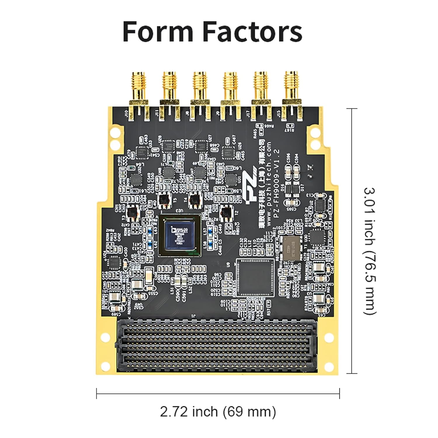
Figure 8.2: Physical dimensions of the PZ-FH9009 FMC Module, showing length and width measurements.
9. Applications
The versatility and high performance of the PZ-FH9009 FMC Module make it suitable for a wide range of advanced applications:

Figure 9.1: Illustrative diagram of potential application areas for the PZ-FH9009 FMC Module.
- Drones: For advanced communication and sensing capabilities.
- Network Security: For signal intelligence and monitoring.
- Spectrum Monitoring: For analyzing and managing radio frequency spectrum.
- Testing & Measurement: As a flexible platform for RF test setups.
- Radar: For prototyping and developing radar systems.
- IoT/M2M: For machine-to-machine communication and Internet of Things applications.
- GPS/GNSS: For advanced positioning and navigation systems.
- Medical: In specialized medical imaging or communication devices.
10. Warranty and Support
Information regarding product warranty and technical support is typically provided by the manufacturer or seller at the time of purchase. Please refer to your purchase documentation or contact SCFPGA directly for details on:
- Warranty period and coverage.
- Technical support contacts and resources.
- Return and repair procedures.
For further assistance, you may also visit the FPGA China seller page on Amazon or the official SCFPGA website (if available).