
1. Product Overview
The SCFPGA PZ7030-SOM-676 and PZ7035-SOM-676 are high-performance System-on-Modules (SOMs) designed for embedded development, edge computing, and industrial automation. These core boards are built on Xilinx ZYNQ-7000 series SoCs (XC7Z030/035), integrating dual-core ARM Cortex-A9 processors with programmable logic (FPGA) in a compact form factor. They are engineered for industrial use, offering robust performance and flexible peripheral integration.
Key Features:
- High-Performance ZYNQ SoC: Features XC7Z030 or XC7Z035 with Dual-Core ARM Cortex-A9 and up to 275K logic cells for advanced embedded computing applications.
- Reliable Industrial Design: Designed for harsh environments with industrial-grade temperature range (-40°C~+85°C) and stable 5V/3A power input.
- Integrated Memory and Flash: Equipped with 1GB DDR3 on both PS and PL sides (total 2GB), 256Mb QSPI FLASH, and 8GB eMMC for fast startup and storage.
- Flexible I/O Expansion: Offers 24 PS MIOs and 164 PL IOs with adjustable levels (1.8V/2.5V/3.3V), including 8/4 pairs of GTX transceivers for high-speed interfaces.
- Rich Peripheral Interfaces: Onboard Gigabit Ethernet chip, multiple clock sources (33.33MHz, 125MHz, 200MHz), reset key, boot switch, and user LEDs for system interaction.
This image displays the top view of the PZ7035-SOM-676 core board, highlighting its compact design and primary components.
2. Component Identification
This section provides a detailed identification of the key components and interfaces on the core board.

This image illustrates the top side of the core board with various components labeled, including PL Side DDR3, Reset Key, Boot Selection Switch, QSPI Flash, EMMC, PS Side DDR3, Gigabit Ethernet Chip, Voltage Regulation, User LED, Download Indicator, and 125MHz Differential Clock.

This image shows the underside of the core board, highlighting the three 120-pin connectors (J1, J2, J3) for carrier board integration, along with the 200MHz Differential Clock and 33.33MHz Single-ended Clock.
3. Setup Instructions
Follow these general steps to set up your SCFPGA ZYNQ FPGA Core Board:
- Prepare the Carrier Board: Ensure your carrier board is compatible with the PZ7030/PZ7035-SOM-676 and provides the necessary power and interfaces.
- Mount the Core Board: Carefully align the 120-pin connectors (J1, J2, J3) on the core board with the corresponding receptacles on your carrier board. Apply gentle, even pressure to seat the board securely.
- Connect Power: Connect a stable 5V/3A power supply to your carrier board. Verify that the power indicator LED on the carrier board (if present) illuminates.
- Configure Boot Mode: Use the onboard boot selection switch (refer to Figure 2) to select the desired startup mode (e.g., JTAG, QSPI, SD card). Consult your carrier board documentation for specific boot configurations.
- Connect Peripherals: Connect any necessary peripherals such as JTAG debugger, Ethernet cable, or other I/O devices to the carrier board.
- Initial Power On: Power on the system. Observe the user LEDs (refer to Figure 2) for initial status indications.
4. Operating Guidelines
This section provides general guidelines for operating the ZYNQ FPGA Core Board.
- Power Supply: Always use a stable 5V/3A power supply. Unstable power can lead to unpredictable behavior or damage.
- Temperature Management: The board is designed for industrial-grade temperatures (-40°C to +85°C). Ensure adequate airflow or heat dissipation, especially during high-load operations, to maintain optimal performance and longevity.
- Software Development: Utilize Xilinx Vivado Design Suite and SDK for developing applications for the ZYNQ SoC. Refer to Xilinx documentation for detailed programming instructions.
- Boot Modes: The board supports JTAG, QSPI, and SD card boot modes. Select the appropriate mode using the onboard switch based on your development or deployment needs.
- I/O Voltage Levels: Be mindful of the adjustable I/O voltage levels (1.8V/2.5V/3.3V) for PL IOs. Ensure compatibility with connected external devices to prevent damage.
- Gigabit Ethernet: The onboard Gigabit Ethernet chip provides network connectivity. Configure network settings through the ARM processor.
5. Maintenance
Proper maintenance ensures the longevity and reliable operation of your core board.
- Cleaning: Keep the board free from dust and debris. Use a soft, dry brush or compressed air for cleaning. Avoid using liquids or solvents.
- Handling: Always handle the board by its edges to avoid touching components, especially the connectors and the ZYNQ SoC. Use anti-static precautions (e.g., anti-static wrist strap) to prevent electrostatic discharge (ESD) damage.
- Storage: When not in use, store the board in an anti-static bag in a cool, dry environment.
- Firmware Updates: Regularly check for firmware and software updates from SCFPGA or Xilinx to ensure optimal performance and security.
6. Troubleshooting
This section addresses common issues you might encounter and provides potential solutions.
- Board does not power on:
- Verify the 5V/3A power supply is correctly connected and functional.
- Check all connections between the core board and the carrier board for proper seating.
- Ensure the power switch on the carrier board (if any) is in the ON position.
- No output from I/O pins:
- Confirm that the I/O voltage levels are correctly configured for your application.
- Check your FPGA design for correct pin assignments and logic.
- Ensure external connections to I/O pins are secure and correctly wired.
- JTAG debugger not detecting the device:
- Ensure the JTAG cable is properly connected to both the board and the host PC.
- Verify that the boot selection switch is set to JTAG mode.
- Check if the JTAG drivers are correctly installed on your host PC.
- Ethernet connection issues:
- Confirm the Ethernet cable is securely connected.
- Check network configurations within your embedded software.
- Verify that the Gigabit Ethernet chip is properly initialized in your design.
If issues persist, refer to the detailed documentation provided by Xilinx for the ZYNQ-7000 series or contact SCFPGA support.
7. Specifications
Detailed technical specifications for the PZ7030-SOM-676 and PZ7035-SOM-676 core boards.

This table provides a side-by-side comparison of the key specifications for both the PZ7030-SOM-676 and PZ7035-SOM-676 models, including FPGA chip, processor core, logic cells, memory, and I/O details.
General Specifications:
| Feature | Description |
|---|---|
| Brand | SCFPGA |
| Model Numbers | PZ7030-SOM-676 / PZ7035-SOM-676 |
| RAM Memory Installed Size | 2 GB (1GB PS side, 1GB PL side) |
| RAM Memory Technology | DDR3 |
| Included Components | ZYNQ core board |
| Built-In Media | 256Mb QSPI FLASH, 8GB eMMC |
| Power Input | 5V/3A |
| Operating Temperature | -40°C to +85°C (Industrial Grade) |
Physical Dimensions:

This image details the physical dimensions of the core board: 83.8mm (3.30 inches) in length and 64.8mm (2.55 inches) in width. It also indicates the top MAX height (3mm), PCB thickness (1.6mm), and connector height (3mm).
8. Package Contents
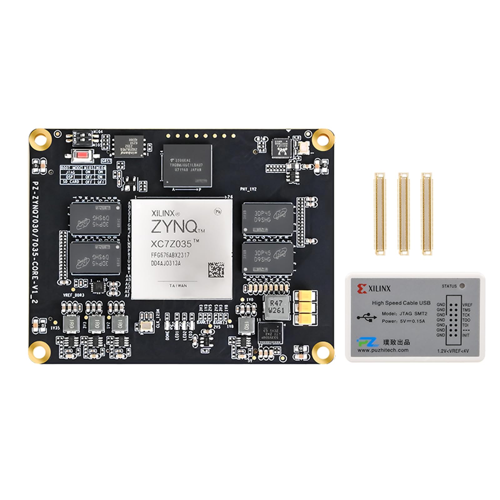
The standard package includes the ZYNQ core board. Optional accessories may be available depending on the specific package purchased.

This image depicts the ZYNQ core board as the primary item. Optional accessories, such as 3 connectors (for the carrier board), a downloader, and a heat dissipation kit (heatsink + DC fan), are also shown as potentially included depending on the package.
For the "Package3 PZ7035-SOM-676" variant, the core board is included. Please check your specific order details for any additional components.
9. Warranty Information
The guarantee period for this product is one (1) year after the delivery of the goods. This warranty covers manufacturing defects under normal use.
The rights of guarantee are invalidated by:
- Unsuitable or unprofessional deployment.
- Normal wear and tear.
- Unsuitable storage conditions.
- Lack of care during utilization.
- Non-approved alterations to the goods made by the client or third parties.
10. Support
For technical assistance, documentation, or further inquiries regarding your SCFPGA ZYNQ FPGA Core Board, please refer to the official SCFPGA website or contact their customer support channels. Ensure you have your product model number and purchase details ready when seeking support.