1. Introduction
The JESSINIE GD32F103C8T6 ARM Core Development Board is a versatile platform designed for embedded systems development. It offers high compatibility with popular microcontroller ecosystems such as STM32, GD32, APM32, and CKS32, ensuring a smooth transition for existing projects. This board features a Type-C interface for modern connectivity and supports high-frequency applications up to 108MHz, alongside integrated peripherals like USB, CAN, and ADC.
This manual provides essential information for setting up, operating, maintaining, and troubleshooting your development board, enabling you to maximize its potential in your projects.
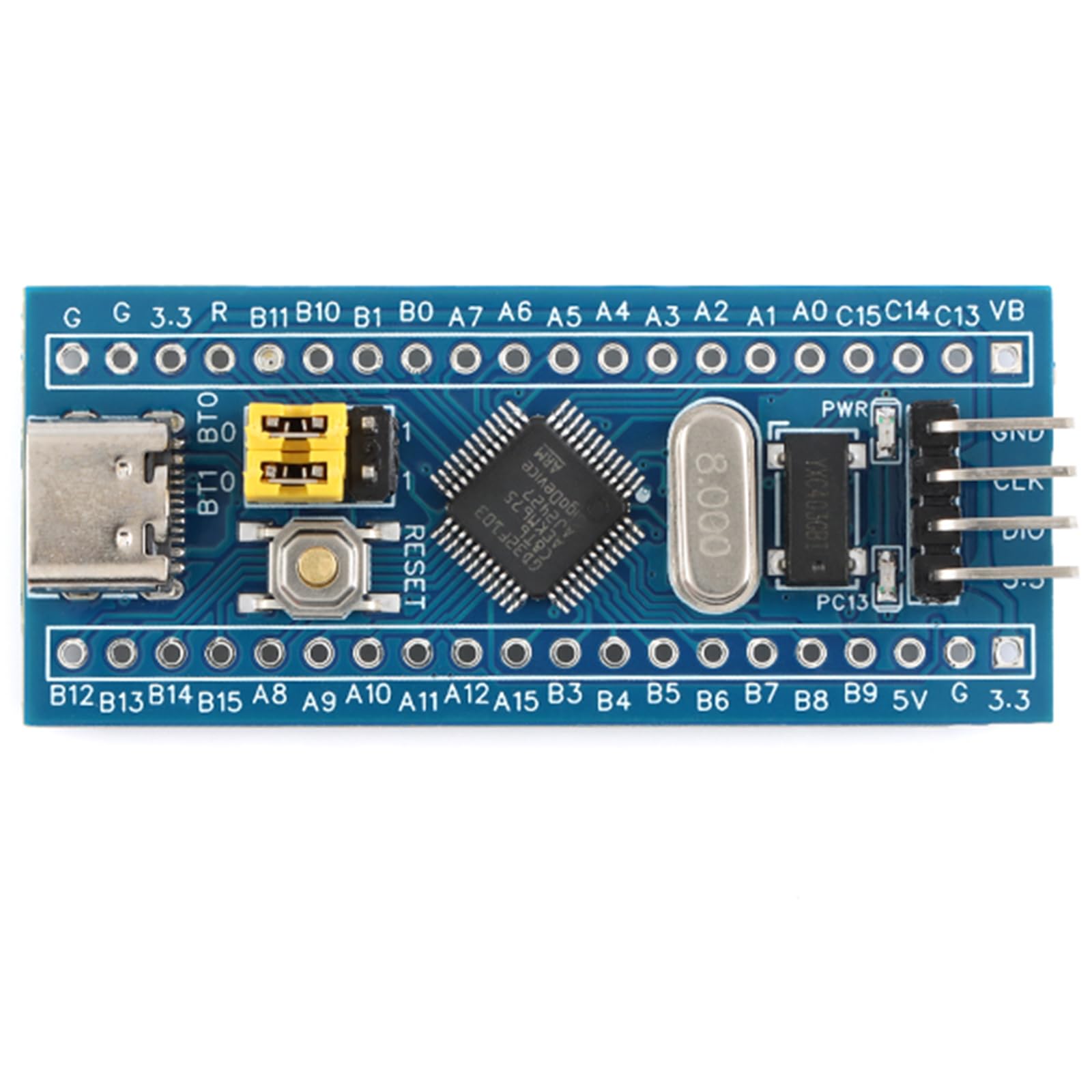
Figure 1: Top view of the GD32F103C8T6 development board, highlighting its compact size of 53mm by 23mm. Key components such as the GD32F103C8T6 microcontroller, USB Type-C port, reset button, BOOT jumpers, and pin headers are visible.
2. Setup Instructions
Follow these steps to prepare your GD32F103C8T6 development board for use:
- Unpacking: Carefully remove the development board from its packaging. Inspect for any visible damage.
- Pin Header Installation: If not already installed, solder the provided pin headers onto the board. This allows for easy integration with breadboards and external components.
- Power Connection: Connect the board to your computer using a standard USB Type-C cable. The board will draw power from the USB port.
- Driver Installation: Your operating system may automatically install necessary drivers. If not, refer to the official GD32 or STM32 documentation for driver installation guides.
- Development Environment Setup: Install your preferred Integrated Development Environment (IDE), such as Keil MDK, STM32CubeIDE, or Arduino IDE with appropriate board support packages.
- Initial Configuration: For programming, ensure the BOOT0 jumper is set correctly. For serial ISP burning, set the BOOT0 jumper to the appropriate position. For SWD/JTAG debugging, ensure the PA13/PB14 SWD debug pins are accessible.

Figure 2: A detailed front view of the GD32F103C8T6 development board, showing the arrangement of the Type-C USB connector, BOOT jumpers, reset button, and the main microcontroller chip. The pin headers for GPIO and power are clearly labeled.
3. Operating Instructions
This section outlines the general operation of the GD32F103C8T6 development board:
- Programming: The board supports programming via SWD/JTAG for debugging and Serial ISP (In-System Programming) through the BOOT0 jumper switch and PA9/PA10 serial burn key interface.
- GPIO Usage: The LQFP48 package provides 37 General Purpose Input/Output (GPIO) pins. Refer to the GD32F103C8T6 datasheet for detailed pinout information and configuration.
- Integrated Peripherals: Utilize the onboard USB, CAN, and ADC interfaces for various applications. Ensure proper library and driver configurations within your development environment.
- Clock Configuration: When running GD32 programs on STM32 frameworks, it may be necessary to adjust the clock initialization code or HSE_STARTUP_TIMEOUT values in your IDE (e.g., Keil) to ensure optimal execution and prevent issues.
- Reset Button: Press the onboard reset button to restart the microcontroller.

Figure 3: This angled perspective of the development board provides a clearer view of the various components and their connections, including the crystal oscillator, power pins, and the general layout, useful for understanding component placement during operation.
4. Maintenance
Proper care and maintenance will extend the lifespan of your development board:
- Handling: Always handle the board by its edges to avoid touching sensitive components or introducing static electricity.
- Cleaning: Use a soft, dry brush or compressed air to remove dust. For stubborn grime, use a lint-free cloth lightly dampened with isopropyl alcohol. Ensure the board is powered off and completely dry before reconnecting.
- Storage: Store the board in an anti-static bag in a cool, dry environment when not in use. Avoid extreme temperatures and humidity.
- Power Supply: Use a stable and appropriate power supply (via USB Type-C) to prevent damage to the board.
5. Troubleshooting
This section addresses common issues you might encounter:
| Issue | Possible Cause / Solution |
|---|---|
| Unrecognized ST-Link device | Ensure your ST-Link utility or IDE is configured to recognize GD/APM/CKS chips as "STM32F103" for debugging. Update ST-Link firmware if necessary. |
| USB enumeration issues | Adjust the clock initialization code in your project for GD32 compatibility. Verify USB cable integrity. |
| Program burning failures (domestic chips) | Utilize the one-touch BOOT0 switching feature to correctly configure the bootloader. Ensure the correct programming method (SWD/JTAG or Serial ISP) is selected. |
| GD32 programs not running optimally on STM32 frameworks | Reduce the clock frequency or adjust HSE_STARTUP_TIMEOUT values in your IDE (e.g., Keil) settings. |
| Board not powering on | Check USB Type-C cable connection and ensure your computer's USB port is functional. Try a different cable or port. |
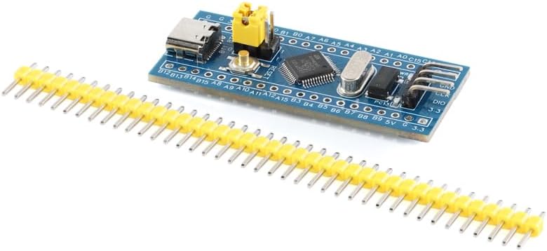
Figure 4: The development board is shown alongside its accompanying pin headers, which users will typically solder onto the board for breadboard compatibility and easier access to GPIOs and other interfaces.
6. Specifications
| Feature | Detail |
|---|---|
| Brand | JESSINIE |
| Model | GD32F103C8T6 |
| Microcontroller | GD32F103C8T6 ARM Core |
| Interface | USB Type-C |
| Compatibility | STM32, GD32, APM32, CKS32 (pin, peripheral, package compatible with STM32F103C8T6) |
| Clock Frequency | Up to 108MHz |
| GPIOs | 37 (LQFP48 package) |
| Integrated Peripherals | USB, CAN, ADC |
| Debugging Support | SWD/JTAG (PA13/PB14 pins) |
| Programming Support | Serial ISP (BOOT0 jumper, PA9/PA10 serial burn key) |
| Item Weight | 2.82 ounces |
| Package Dimensions | 5.91 x 3.94 x 0.47 inches |
| Voltage | 35 Volts (DC) |

Figure 5: The underside of the development board reveals surface-mounted components and traces, providing insight into the board's internal design and power distribution.
7. Warranty Information
JESSINIE warrants this product against defects in materials and workmanship for a period of one (1) year from the original date of purchase. This warranty does not cover damage caused by accident, misuse, abuse, modification, improper installation, or normal wear and tear. Proof of purchase is required for all warranty claims. For warranty service, please contact customer support.
8. Customer Support
For technical assistance, troubleshooting, or general inquiries regarding your JESSINIE GD32F103C8T6 ARM Core Development Board, please refer to the following resources:
- Online Resources: Visit the official JESSINIE website for product documentation, FAQs, and community forums.
- Email Support: Contact our support team at support@jessinie.com. Please include your product model and a detailed description of your issue.
- Community Forums: Engage with other users and experts in online forums dedicated to GD32 and ARM development for shared knowledge and solutions.
