1. Introduction
This manual provides essential information for the proper setup, operation, and maintenance of the Generic MAX2870 RF Signal Generator Module. This module is an ultra-wideband phase-locked loop (PLL) with an integrated voltage-controlled oscillator (VCO), designed to generate RF signals across a broad frequency range.
The MAX2870 module is capable of generating signals from 23.5MHz to 6.0GHz, maintaining excellent phase noise and spurious specifications. It features dual-channel differential output drivers, which can be configured to provide output power from -4dBm to +5dBm. Control is typically achieved via a three-wire SPI interface, and the module operates with a 3.3V pin header power supply or a DC 5V input, utilizing an onboard 3.3V voltage stabilizing IC and a 100MHz reference clock frequency.
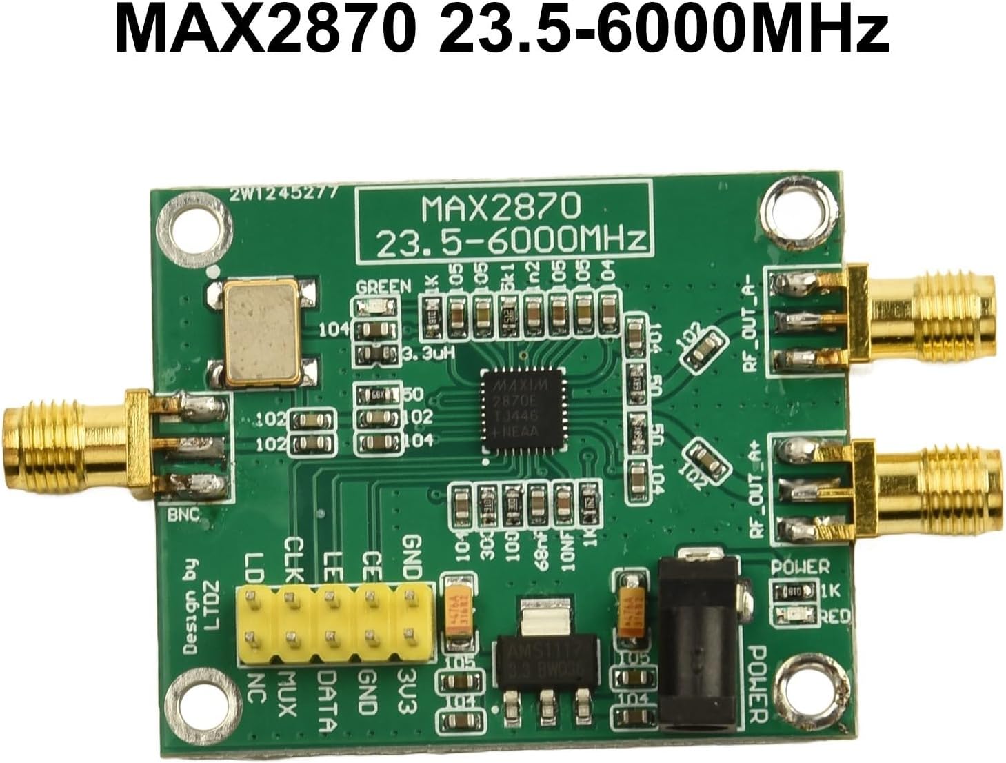
Figure 1: Top-down view of the MAX2870 RF Signal Generator Module, showing the MAX2870 chip, connectors, and various components.
2. Safety Information
Always handle electronic components with care. Observe proper electrostatic discharge (ESD) precautions to prevent damage to the module. Ensure power supply voltages are within the specified range to avoid component failure. This module is intended for use by individuals familiar with electronic circuits and RF systems.
3. Package Contents
Verify that your package contains the following item:
- 1 x MAX2870 RF Signal Generator Module
Note: Additional cables, power supplies, or development boards (e.g., STM32 driver) are typically sold separately and are required for full functionality.
4. Setup
Follow these steps to set up your MAX2870 RF Signal Generator Module:
- Power Supply Connection: Connect a stable power supply to the module. The module can be powered via the 3.3V pin header or a DC 5V input. Ensure the voltage is correct to prevent damage. The onboard 3.3V voltage stabilizing IC regulates the input.
- Control Interface: Connect the module to your control system (e.g., an STM32 microcontroller) using the three-wire SPI interface. The pins are typically labeled CLK (Clock), DATA (MOSI), and LE (Latch Enable). Refer to the module's pinout for exact connections.
- RF Output Connection: Connect your RF measurement equipment or load to the RF output connectors. The module provides dual-channel differential output drivers.
- Reference Clock: The module has an onboard 100MHz reference clock frequency. If an external reference clock is required, consult the MAX2870 datasheet for proper integration.

Figure 2: Example of the MAX2870 module being integrated into a larger electronic system.
5. Operating Instructions
Operating the MAX2870 module involves configuring its internal registers via the SPI interface to achieve the desired output frequency and power level.
5.1. Frequency Generation
The MAX2870 can generate frequencies from 23.5MHz to 6.0GHz. The specific output frequency is set by programming the internal PLL registers. This typically involves calculating the appropriate N and R divider values, along with other PLL parameters, based on the desired output frequency and the 100MHz reference clock.
5.2. Output Power Adjustment
The module's dual-channel differential output drivers allow for individual configuration of output power, ranging from -4dBm to +5dBm. This is controlled by specific register settings within the MAX2870 chip. Refer to the MAX2870 datasheet for detailed register maps and programming sequences.
5.3. SPI Communication Protocol
The module communicates using a standard three-wire SPI protocol. Data is typically sent in 24-bit or 32-bit words, depending on the register being accessed. A typical communication sequence involves:
- Setting the Latch Enable (LE) pin low.
- Shifting data bits (clocked by CLK) into the DATA pin.
- Setting the LE pin high to latch the data into the MAX2870's internal registers.
Consult the MAX2870 datasheet for precise timing diagrams and register definitions.
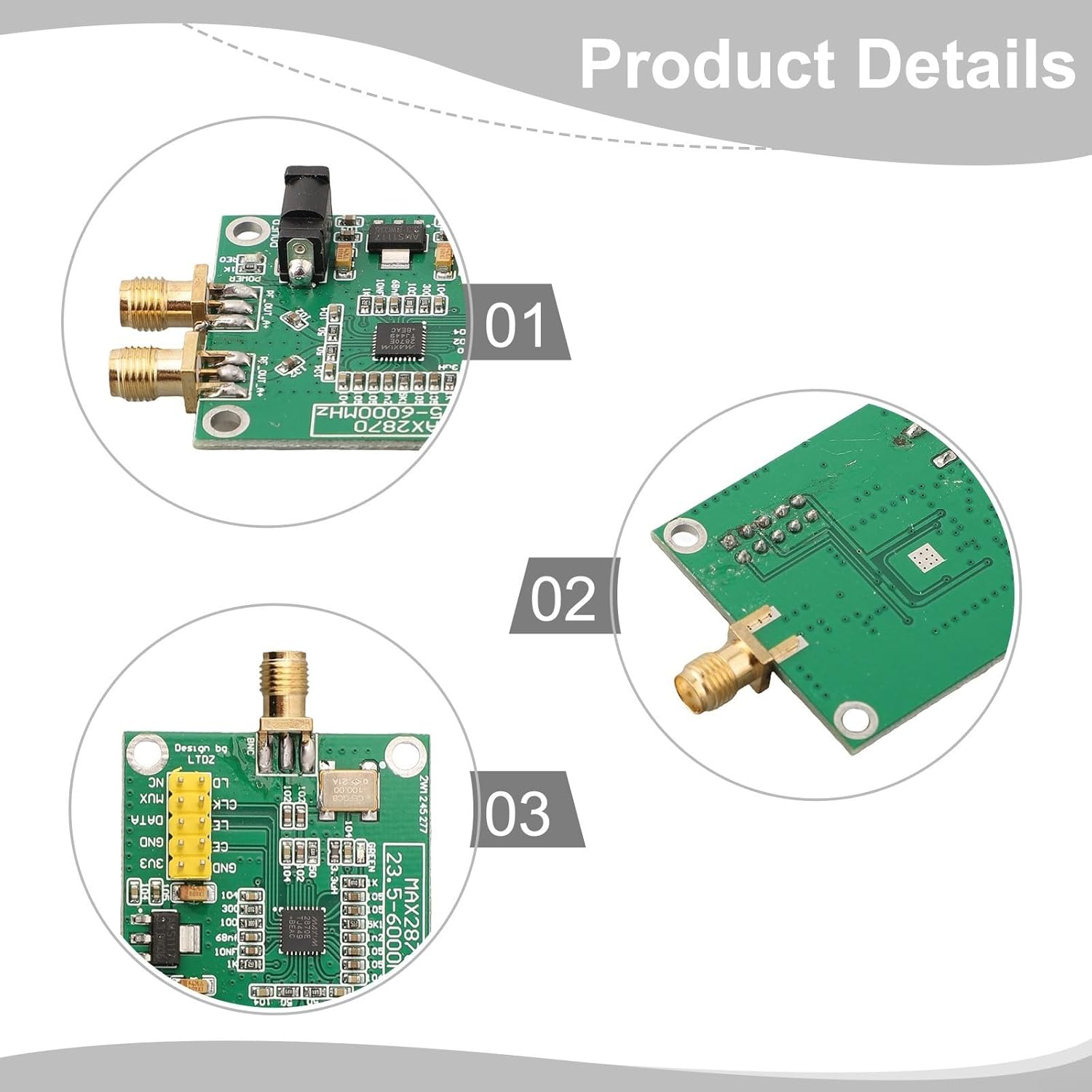
Figure 3: Detailed views of the MAX2870 module, showing various connection points and integrated circuits.
6. Maintenance
The MAX2870 RF Signal Generator Module is designed for reliability and requires minimal maintenance. To ensure optimal performance and longevity:
- Cleaning: Keep the module clean and free from dust and debris. Use a soft, dry cloth for cleaning. Avoid using liquids or abrasive cleaners.
- Storage: Store the module in a dry, cool environment, away from direct sunlight and extreme temperatures.
- Handling: Always handle the module by its edges to avoid touching sensitive components. Continue to observe ESD precautions.
- Inspection: Periodically inspect the connectors and solder joints for any signs of damage or wear.

Figure 4: Angled view of the MAX2870 module, illustrating its compact design and connector layout.
7. Troubleshooting
If you encounter issues with your MAX2870 module, consider the following troubleshooting steps:
- No Power:
- Verify that the power supply is correctly connected and providing the specified voltage (3.3V or 5V DC).
- Check for proper polarity of the power connection.
- No RF Output:
- Ensure the module is correctly powered and the control system is active.
- Check the SPI communication for errors. Verify that the correct register values are being written to the MAX2870.
- Confirm that the RF output connectors are securely attached to the load or measurement equipment.
- Review the MAX2870 datasheet to ensure all necessary registers are configured for output enable and desired frequency.
- Incorrect Frequency/Power:
- Double-check your SPI programming sequence and the calculated register values for frequency and power settings.
- Ensure the 100MHz reference clock is stable and accurate.
- Verify that the control system's clock and data lines are correctly connected and functioning.
- Module Not Responding to SPI:
- Check all SPI connections (CLK, DATA, LE, GND) for continuity and correct wiring.
- Ensure the control system's SPI peripheral is correctly configured (e.g., clock polarity, phase).
For complex issues, refer to the official Analog Devices (formerly Maxim Integrated) MAX2870 datasheet and application notes for in-depth technical details and programming guidance.
8. Specifications
| Feature | Specification |
|---|---|
| Model Number | 1226191 |
| Frequency Range | 23.5 MHz to 6.0 GHz |
| Output Power Range | -4 dBm to +5 dBm (configurable) |
| Control Interface | 3-wire SPI |
| Power Supply | 3.3V (pin header) or 5V DC (onboard 3.3V regulator) |
| Reference Clock | 100 MHz (onboard) |
| Dimensions (L x W x H) | 65mm x 37mm x 12mm (approx. 2.56 x 1.46 x 0.47 inches) |
| Weight | Approx. 1.06 ounces (30 grams) |
| Integrated Components | MAX2870 PLL/VCO |
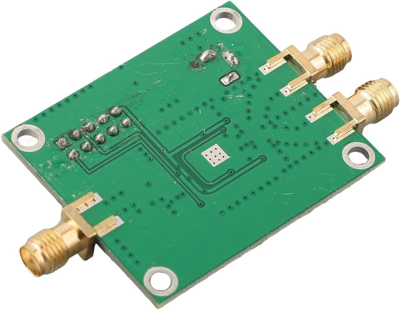
Figure 5: Bottom view of the MAX2870 module, revealing the PCB layout and unpopulated components.
9. Warranty and Support
Specific warranty terms and support details for this Generic MAX2870 RF Signal Generator Module are typically provided by the seller at the time of purchase. Please refer to your purchase documentation or contact the seller directly for information regarding warranty coverage, returns, and technical support.
For detailed technical specifications and advanced programming information related to the MAX2870 integrated circuit, please consult the official datasheet provided by Analog Devices (formerly Maxim Integrated).
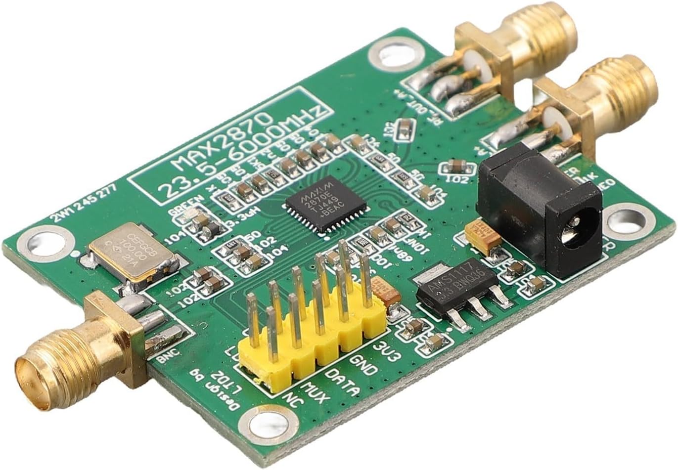
Figure 6: Angled view of the MAX2870 module, highlighting the SPI control pins and power input jack.


