1. Introduction
The Generic PCA9306 I2C Level Translator Breakout Board is designed to facilitate communication between devices operating at different voltage levels. This module is a dual bidirectional voltage-level translator, essential for systems where components utilize varying voltage standards for I2C-bus and SMBus communication.
It supports low-side operation from 1.0 V to 3.6 V and high-side operation from 1.8 V to 5.5 V. By simply applying the appropriate low- and high-side reference voltages to the VREF1 and VREF2 pins, and connecting your I/O, the board enables seamless bidirectional voltage translation without requiring a dedicated direction pin.
2. Key Features
- Dual Bidirectional Translation: Functions as a 2-bit bidirectional translator for SDA and SCL lines, suitable for mixed-mode I2C-bus applications.
- I2C/SMBus Compatibility: Compatible with Standard-mode, Fast-mode, and Fast-mode Plus I2C-bus and SMBus protocols.
- Low Propagation Delay: Features less than 1.5 ns propagation delay, accommodating Standard-mode and Fast-mode I2C-bus devices.
- Wide Voltage Translation Range: Supports various voltage level translations, including:
- 1.0 V Vref(1) to 1.8 V, 2.5 V, 3.3 V, or 5 V Vbias
- 1.2 V Vref(1) to 1.8 V, 2.5 V, 3.3 V, or 5 V Vbias
- 1.8 V Vref(1) to 3.3 V or 5 V Vbias
- 2.5 V Vref(1) to 5 V Vbias
- 3.3 V Vref(1) to 5 V Vbias
- No Direction Pin Required: Simplifies integration by providing bidirectional voltage translation without the need for an external direction control pin.
- Low ON-State Connection: A low 3.5 Ω ON-state connection between input and output ports minimizes signal distortion.
3. Setup and Connection
The PCA9306 breakout board is designed for straightforward integration into your electronic projects. Below are the general steps and pin descriptions for proper setup.
3.1 Pinout Diagram
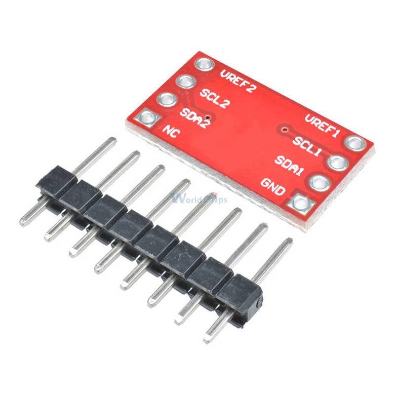
Figure 1: Back view of the PCA9306 breakout board, illustrating the pin labels for connection.
The board features two sets of I2C lines (SDA1/SCL1 and SDA2/SCL2) and two reference voltage inputs (VREF1 and VREF2), along with a ground (GND) pin and an NC (No Connection) pin.
3.2 Connection Steps
- Connect Low-Side Reference Voltage (VREF1): Connect the voltage of your low-voltage I2C device (e.g., 1.8V, 2.5V, 3.3V) to the VREF1 pin. This sets the reference for the low-voltage side.
- Connect High-Side Reference Voltage (VREF2): Connect the voltage of your high-voltage I2C device (e.g., 3.3V, 5V) to the VREF2 pin. This sets the reference for the high-voltage side.
- Connect Ground (GND): Ensure a common ground connection between the PCA9306 board and both your low-voltage and high-voltage devices.
- Connect Low-Side I2C (SDA1, SCL1): Connect the SDA (Serial Data) and SCL (Serial Clock) lines from your low-voltage I2C device to the SDA1 and SCL1 pins, respectively.
- Connect High-Side I2C (SDA2, SCL2): Connect the SDA and SCL lines from your high-voltage I2C device to the SDA2 and SCL2 pins, respectively.
- Enable Pin: The PCA9306 typically has an internal pull-up on its enable pin. To activate the translation, ensure the enable pin is driven high. On this breakout board, the enable pin is usually tied high or configured to be always enabled, simplifying usage. Refer to the specific board's schematic if unsure.

Figure 2: PCA9306 breakout board with included header pins, ready for integration into a breadboard or custom PCB.
4. Operation
Once correctly wired, the PCA9306 operates transparently as a voltage level translator for your I2C communication. It automatically handles the bidirectional data flow between the two voltage domains.
The key to its operation is the application of the correct reference voltages (VREF1 and VREF2) which define the voltage levels for the low and high sides of the translation. The internal circuitry of the PCA9306 adjusts the signal levels on the SDA and SCL lines to match the respective voltage domains, allowing seamless data exchange.
No software configuration or additional control signals are typically required beyond providing the correct power and ground connections and the I2C lines.
5. Technical Specifications
| Parameter | Value |
|---|---|
| Model | PCA9306 |
| Type | Level Translator Breakout Board |
| Low-Side Voltage (VREF1) Range | 1.0 V to 3.6 V |
| High-Side Voltage (VREF2) Range | 1.8 V to 5.5 V |
| Bidirectional Channels | 2 (SDA, SCL) |
| I2C Bus Compatibility | Standard-mode, Fast-mode, Fast-mode Plus |
| SMBus Compatibility | Yes |
| ON-State Connection Resistance | 3.5 Ω (typical) |
| Color | Red PCB |
6. Troubleshooting
If you encounter issues while using the PCA9306 level translator, consider the following common troubleshooting steps:
- No Communication:
- Verify that VREF1 and VREF2 are correctly supplied with the appropriate voltages for your low-side and high-side devices.
- Ensure a common ground connection between all devices (PCA9306, low-voltage device, high-voltage device).
- Check all I2C connections (SDA1, SCL1, SDA2, SCL2) for proper wiring and continuity.
- Confirm that the enable pin (if exposed and not internally tied high) is correctly driven high.
- Incorrect Voltage Levels:
- Measure the voltages at VREF1 and VREF2 to ensure they match the requirements of your connected devices.
- Use an oscilloscope to check the signal levels on SDA and SCL lines on both sides of the translator to confirm proper translation.
- Intermittent Communication:
- Ensure adequate power supply stability for both voltage domains.
- Check for loose connections or cold solder joints.
- Verify that the I2C pull-up resistors are correctly implemented on both sides of the bus, if not already integrated into your devices or the breakout board.
7. Maintenance
The PCA9306 breakout board is a robust electronic component and requires minimal maintenance. To ensure its longevity and reliable operation:
- Keep Clean: Avoid dust, dirt, and moisture accumulation on the board. If cleaning is necessary, use a soft, dry brush or compressed air. Do not use liquid cleaners unless specifically designed for electronics and applied sparingly.
- Handle with Care: Avoid physical stress, bending, or dropping the board. Static electricity can damage electronic components; handle the board in an ESD-safe environment.
- Proper Storage: When not in use, store the board in an anti-static bag in a cool, dry place away from direct sunlight and extreme temperatures.

