1. Introduction
The Gikfun SMD/SMT Practice PCB Board is designed for electronic learners and students to develop and refine their surface-mount device (SMD) and surface-mount technology (SMT) soldering skills. This DIY kit provides a practical platform for assembling and soldering various electronic components, making it an ideal tool for educational purposes and hands-on training.
This manual provides essential information for the proper assembly, operation, and maintenance of your Gikfun practice board. Please read it thoroughly before beginning your soldering project.
2. Safety Information
Always prioritize safety when working with soldering equipment. Failure to follow safety guidelines can result in injury or damage to components.
- Ventilation: Work in a well-ventilated area to avoid inhaling solder fumes. Use a fume extractor if available.
- Eye Protection: Always wear safety glasses to protect your eyes from splashes of molten solder or flying debris.
- Burn Hazard: Soldering irons reach high temperatures. Avoid direct contact with the tip and allow components to cool before handling.
- Electrical Safety: Ensure your soldering iron and other tools are in good working condition and properly grounded. Do not work with live circuits.
- First Aid: Keep a first aid kit nearby for minor burns or cuts.
- Cleanliness: Keep your workspace clean and free of flammable materials.
3. Package Contents
Verify that all components listed below are present in your kit:
- 1x Practice PCB Board
- Assorted SMD/SMT electronic components (resistors, capacitors, diodes, ICs, etc.)

Image 3.1: Overview of the Gikfun SMD/SMT Practice PCB Board and its accompanying components, including various resistors, capacitors, diodes, and integrated circuits, laid out on a white surface.
4. Setup
Before you begin soldering, ensure your workspace is prepared and you have the necessary tools.
4.1 Required Tools (Not Included)
- Soldering Iron with fine tip
- Solder wire (preferably lead-free with flux core)
- Tweezers (fine-tip for SMD components)
- Magnifying glass or microscope (recommended for small components)
- Solder wick or desoldering pump
- Isopropyl alcohol and cotton swabs for cleaning
4.2 Preparing the PCB and Components
- Unpack the PCB and components. Handle the PCB by its edges to avoid touching the copper traces.
- Organize your components. The PCB is clearly marked with component designators (e.g., R1, C1, D1) and component types.
- Ensure your soldering iron is heated to the appropriate temperature for your solder type (typically 300-350°C for lead-free solder).

Image 4.1: A hand holding the Gikfun SMD/SMT Practice PCB Board, showcasing the layout and some of the small surface-mount components ready for assembly.
5. Operating Instructions: Soldering Process
This section outlines the general steps for soldering SMD components onto the practice board. Refer to the component identification section for specific component types.
5.1 General Soldering Steps
- Tin one pad: Apply a small amount of solder to one of the pads where the component will be placed.
- Position component: Using tweezers, carefully place the SMD component onto its designated pads. While holding the component in place, reheat the tinned pad with your soldering iron. The component should settle into the molten solder.
- Solder second pad: Once the first side is secured, solder the remaining pads. Apply the soldering iron tip to the component lead and the pad simultaneously, then feed a small amount of solder to the joint. Remove the solder, then the iron.
- Inspect: Visually inspect each solder joint for proper formation. Look for smooth, shiny, concave fillets. Avoid cold joints (dull, lumpy) or solder bridges (solder connecting two adjacent pads).
- Clean: After soldering, clean any flux residue from the board using isopropyl alcohol and a cotton swab.
Important: Ensure all components are placed in the correct direction and location. Pay close attention to polarity for diodes and integrated circuits. Check for pseudo and float welding, as this is critical for successful practice and testing.

Image 5.1: A detailed view of the red Gikfun SMD/SMT Practice PCB Board, showing various surface-mount components successfully soldered onto their respective pads, demonstrating proper soldering technique.
6. Component Identification
The Gikfun practice board features clearly marked areas for different types and sizes of SMD components. Familiarize yourself with these markings to ensure correct placement.
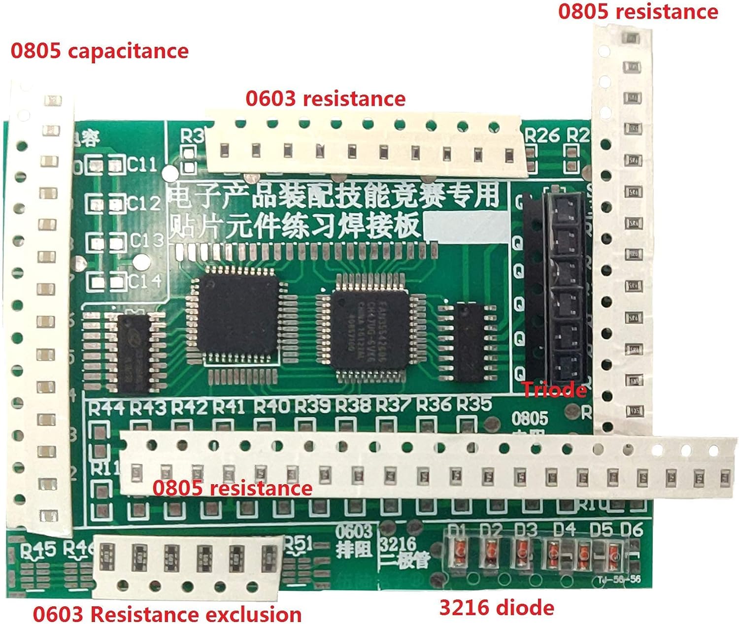
Image 6.1: The Gikfun SMD/SMT Practice PCB Board with various component types and sizes clearly labeled, including 0805 capacitance, 0603 resistance, 0805 resistance, triode, and 3216 diode, aiding in component identification and placement.
- Resistors (R): Typically marked with 'R' followed by a number (e.g., R1, R2). Common sizes include 0603 and 0805.
- Capacitors (C): Marked with 'C' followed by a number (e.g., C1, C2). Common sizes include 0805.
- Diodes (D): Marked with 'D' followed by a number (e.g., D1, D2). Pay attention to polarity (cathode band). Common types include 3216 diodes.
- Transistors/Triodes (Q): Marked with 'Q' followed by a number (e.g., Q1, Q2).
- Integrated Circuits (IC/U): Marked with 'U' or 'IC' followed by a number. These often have a dot or notch indicating pin 1 for correct orientation.
The PCB itself has silkscreen markings indicating the footprint and sometimes the value or type of component to be placed. Always cross-reference the physical component with the PCB markings.
7. Maintenance
Proper care and maintenance will ensure the longevity of your practice board and tools.
- Cleaning the PCB: After soldering, use isopropyl alcohol to clean any remaining flux residue from the board. This prevents corrosion and ensures a clean appearance.
- Soldering Iron Care: Keep your soldering iron tip clean by wiping it on a damp sponge or brass wool regularly. Tin the tip with a fresh layer of solder before storing.
- Storage: Store the practice board and unused components in a dry, dust-free environment.
8. Troubleshooting Common Soldering Issues
Encountering issues is part of the learning process. Here are some common problems and their solutions:
| Problem | Possible Cause | Solution |
|---|---|---|
| Cold Solder Joint (dull, lumpy, poor connection) | Insufficient heat, component movement during cooling. | Reheat the joint, apply fresh solder, and ensure the component remains still until the solder solidifies. |
| Solder Bridge (solder connecting two adjacent pads) | Too much solder, incorrect iron technique. | Use solder wick or a desoldering pump to remove excess solder. Clean the area and re-solder if necessary. |
| Lifted Pad (copper pad detaches from PCB) | Excessive heat or force applied to the pad. | This is difficult to repair. Try to carefully re-attach with adhesive or run a thin wire to an adjacent trace if possible. Avoid excessive heat in the future. |
| Component Not Sticking | Pads not tinned, insufficient heat, oxidized pads. | Ensure pads are clean and tinned. Increase iron temperature slightly if safe. |
9. Specifications
- Brand: Gikfun
- Model: B09PH85639
- Included Components: Practice PCB Board, Assorted SMD/SMT Components
- Application: SMD/SMT Soldering Skill Training, Electronic Learning

Image 9.1: A red Gikfun SMD/SMT Practice PCB Board featuring ruler markings for component size reference, surrounded by various surface-mount components, illustrating the board's design for practical training.
10. Warranty and Support
This product is intended as a DIY practice kit. Due to the nature of DIY electronics and soldering, specific warranties on individual components or the assembled product are not typically offered. However, Gikfun strives for customer satisfaction.
For any questions regarding missing parts, defects upon arrival, or general inquiries, please contact Gikfun customer support through the retailer where the product was purchased or visit the official Gikfun store online: Gikfun Official Store.