1. Introduction
This manual provides essential information for the proper use and understanding of the Aexit 7x9cm Single-Sided Universal PCB Prototyping Boards. These boards are designed for building prototypes of electronic circuits, offering a flexible platform for component placement and soldering.
2. Product Overview
The Aexit Universal PCB Boards are single-sided circuit boards featuring a grid of pre-drilled holes, ideal for hobbyists, students, and professionals to construct custom electronic circuits. Each board includes referencing numbers printed along the edges for easy identification of individual holes, facilitating precise component placement.
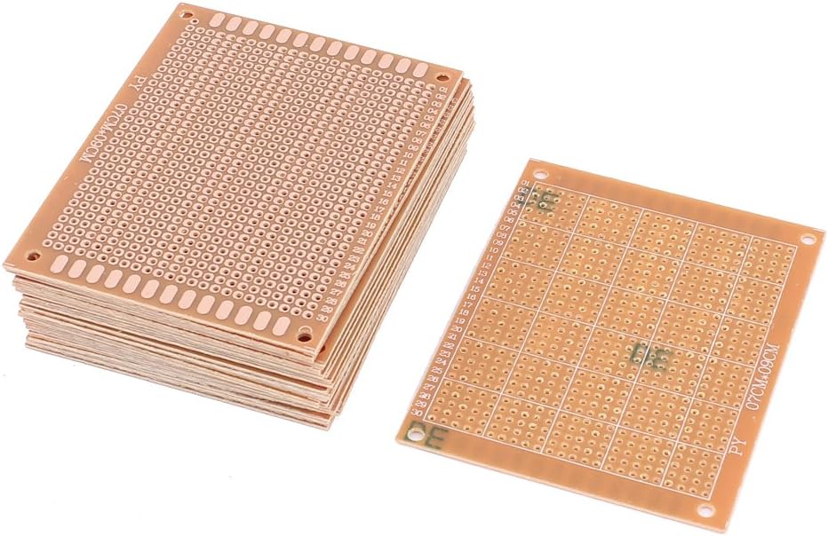
Figure 1: A stack of Aexit universal PCB boards, alongside a single board laid flat. The boards feature a grid of pre-drilled holes and numbered references along the edges, indicating their layout for electronic component placement.
Key Features:
- Single-Sided Design: Facilitates easy soldering and component mounting.
- Pre-drilled Holes: Standard 1mm diameter holes with 2.54mm (0.1") pitch for compatibility with most electronic components.
- Numbered References: Grid coordinates printed on four sides for precise component placement and circuit tracing.
- Durable Material: Constructed from FR-4 (Glass Fiber) with copper traces for reliability.
- Standard Size: Each board measures approximately 7 x 9 cm (2.8" x 3.5").
3. Setup and Preparation
- Inspection: Before use, visually inspect each PCB board for any manufacturing defects or damage.
- Workspace Preparation: Ensure a clean, well-lit, and ventilated workspace. Gather necessary tools such as a soldering iron, solder, desoldering wick/pump, wire cutters, pliers, and safety glasses.
- Component Layout Planning: Plan your circuit layout on paper or using a breadboard first. Utilize the numbered grid on the PCB for accurate component placement.
4. Operating Instructions
- Component Insertion: Insert components into the desired holes on the PCB. Ensure the component leads pass through the holes completely.
- Soldering: Heat the component lead and the copper pad simultaneously with the soldering iron. Apply a small amount of solder to the heated joint, allowing it to flow evenly around the lead and pad. Remove the soldering iron and allow the joint to cool.
- Lead Trimming: After soldering, use wire cutters to trim any excess component leads close to the solder joint.
- Creating Connections: Use jumper wires or solder bridges to create electrical connections between different points on the board as per your circuit design. The 2.54mm pitch allows for standard header pins and ICs.
- Testing: After assembly, thoroughly test your circuit for functionality and continuity before applying power.
5. Maintenance
- Storage: Store unused PCB boards in a dry, dust-free environment to prevent oxidation of the copper pads.
- Cleaning: If necessary, clean the boards with isopropyl alcohol and a soft brush to remove flux residue after soldering. Ensure the board is completely dry before use or storage.
6. Troubleshooting
- Poor Solder Joints: If a component is not making proper contact, re-heat the joint and apply fresh solder. Ensure the soldering iron tip is clean and properly tinned.
- Solder Bridges: Accidental connections between adjacent pads can cause short circuits. Use desoldering wick or a desoldering pump to remove excess solder.
- Component Orientation: Always double-check the orientation of polarized components (e.g., diodes, electrolytic capacitors, ICs) before soldering.
7. Specifications
| Attribute | Value |
|---|---|
| Product Name | Universal PCB Board |
| Board Hole Diameter | 1mm / 0.039" |
| Board Hole Pitch | 2.54mm / 0.1" |
| Mount Hole Diameter | 3mm / 0.12" |
| Mount Hole Center Distance | 82 x 61mm / 3.2" x 2.4" (L*W) |
| Size (Approx.) | 7 x 9cm / 2.8" x 3.5" (W*L) |
| Thickness (Approx.) | 1.2mm / 0.047" |
| Material | FR-4 (Glass Fiber), Copper |
| Color | Copper Tone |
| Weight (per board, approx.) | 8.65g (173g for 20 boards) |
8. Support
For technical assistance or inquiries regarding the Aexit Universal PCB Prototyping Boards, please refer to the seller's support channels or contact the manufacturer directly. Ensure you have your product details available when seeking support.