Introduction
This manual provides essential information for the proper use and care of your Aexit Single Sided Prototyping Boards. These boards are designed for building prototypes of electronic circuits, offering a convenient platform for testing and developing your designs.
The boards feature referencing letters printed on one side, facilitating easy identification and organization of individual holes during circuit assembly.
Product Features
- Universal PCB Board: Suitable for a wide range of electronic prototyping applications.
- Single-Sided Design: Efficient for basic circuit layouts.
- Pre-drilled Holes: Standard 1mm diameter holes with 2.54mm pitch for easy component insertion.
- Referencing Letters: Printed on one side for organized component placement and circuit tracing.
- Durable Construction: Made from quality materials for reliable use.
Setup
The Aexit Prototyping Boards are ready for immediate use. No complex assembly is required. Follow these steps to prepare your workspace:
- Prepare Workspace: Ensure your work area is clean, well-lit, and free from static electricity.
- Gather Tools: Have your soldering iron, solder, wire cutters, wire strippers, and electronic components ready.
- Inspect Board: Before starting, visually inspect the prototyping board for any physical damage or manufacturing defects.
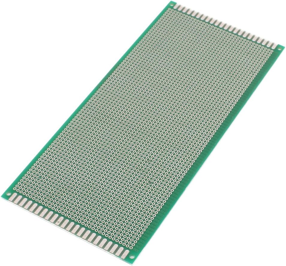
Image 1: Top view of the prototyping board, displaying the grid of solder pads.
Operating Instructions
Using the prototyping board involves placing and soldering electronic components to create a circuit. Here are general guidelines:
- Design Your Circuit: Before soldering, plan your circuit layout. You may use a breadboard for initial testing.
- Component Placement: Insert component leads into the desired holes on the board. The 2.54mm (0.1 inch) pitch is standard for most through-hole components.
- Soldering: Carefully solder the component leads to the copper pads on the underside of the board. Ensure good solder joints for reliable connections.
- Wiring Connections: Use jumper wires or component leads to create connections between different points on the board. The referencing letters (A, B, C, etc.) and numbers along the edges can help in identifying specific points.
- Testing: After assembly, thoroughly test your circuit to ensure it functions as intended.

Image 2: Angled view of the prototyping board, highlighting the solder pads and edge connections.
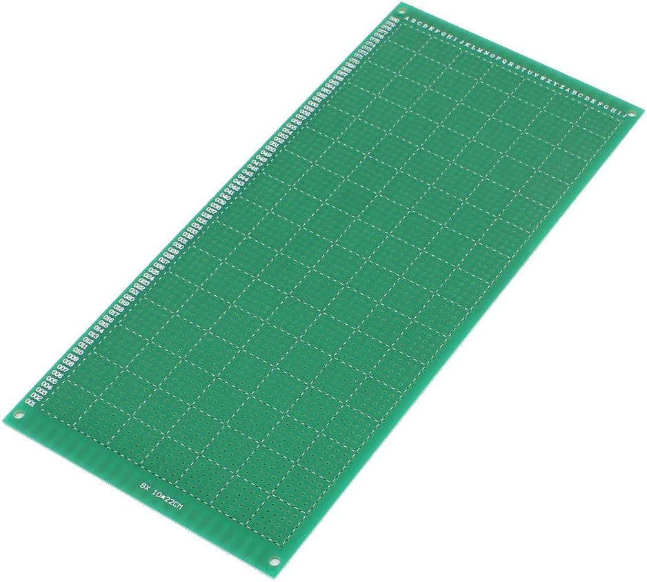
Image 3: Underside view of the prototyping board, showing the referencing letters and numbers.
Maintenance
These prototyping boards require minimal maintenance. Proper handling and storage will ensure their longevity and usability.
- Cleaning: If necessary, gently clean the board with isopropyl alcohol and a soft brush to remove flux residue after soldering. Ensure the board is completely dry before use.
- Storage: Store unused boards in a dry, dust-free environment, preferably in anti-static bags, to prevent oxidation of the copper pads and accumulation of debris.
- Handling: Avoid bending or applying excessive force to the boards, as this can damage the traces or the board material.
Troubleshooting
Most issues encountered with prototyping boards are related to soldering or circuit design. The board itself is a passive component and rarely malfunctions.
- Poor Connections: If your circuit is not working, check all solder joints for cold joints or bridges. Re-solder as necessary.
- Component Orientation: Ensure polarized components (diodes, LEDs, electrolytic capacitors, ICs) are inserted with the correct orientation.
- Circuit Design Errors: Double-check your circuit schematic against your physical layout.
- Short Circuits: Inspect the board for unintended solder bridges or stray wire strands that could be causing short circuits.

Image 4: Close-up of the board's edge, showing detailed numbering for reference.
Specifications
| Feature | Detail |
|---|---|
| Product Name | Universal PCB Board |
| Hole Diameter | Approximately 1mm (0.04") |
| Hole Pitch | Approximately 2.54mm (0.1") |
| Board Dimensions (W x L) | Approximately 10 x 22cm (4" x 8.8") |
| Thickness | Approximately 1mm (0.04") |
| Color | Green |
| Weight (per board) | Approximately 67g |
| Material | PCB (Printed Circuit Board) |
Warranty and Support
Aexit prototyping boards are designed for reliability. As these are passive components used in custom circuit development, specific warranties may vary depending on the retailer and purchase conditions. For any product-related inquiries or support, please refer to the vendor or retailer from whom the product was purchased.
For general information about Aexit products, you may visit the Aexit brand page on Amazon.