
SINGARE DLB01
Instruction Manual: 50 Pcs Double Sided PCB Board Prototype Kit
Model: DLB01
1. Product Overview
The SINGARE 50 Pcs Double Sided PCB Board Prototype Kit is designed for DIY electronics enthusiasts and professionals. This universal printed circuit board kit provides a versatile platform for soldering and prototyping electronic circuits. The double-sided design allows for more complex circuit layouts and easier component mounting.

Image 1.1: A comprehensive view of the 50-piece double-sided PCB board prototype kit, showcasing the different sizes included in the package.
2. Package Contents
Each kit contains a total of 50 double-sided prototype PCB universal boards, distributed across five different dimensions to accommodate various project needs. The boards are made from high-quality FR4 glass fiber with a green basic color and silver tone pads.
- 20 pieces of 2x8CM prototype PCB universal board
- 12 pieces of 3x7CM prototype PCB universal board
- 10 pieces of 4x6CM prototype PCB universal board
- 6 pieces of 5x7CM prototype PCB universal board
- 2 pieces of 6x8CM prototype PCB universal board
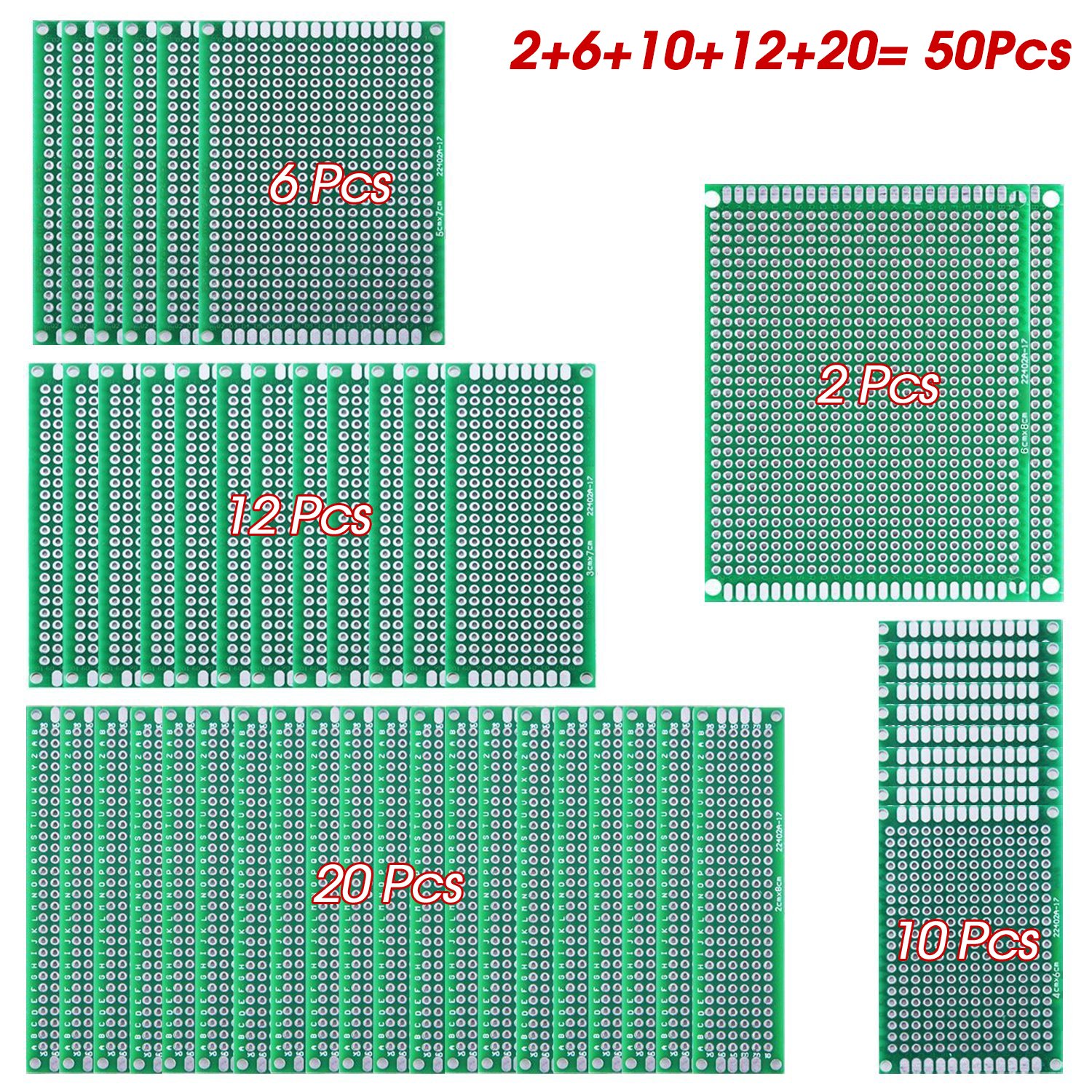
Image 2.1: An illustration detailing the quantity breakdown for each size of PCB board included in the 50-piece kit.
3. Specifications
| Feature | Detail |
|---|---|
| Material | High-quality FR4 Glass Fiber |
| Board Thickness | Approximately 1.6mm |
| Color | Green basic with silver tone pads |
| Board Types Included | 2x8CM, 3x7CM, 4x6CM, 5x7CM, 6x8CM |
| Total Quantity | 50 pieces |
| Model Number | DLB01 |
| Package Dimensions | 6.54 x 4.53 x 0.67 inches |
| Item Weight | 0.16 ounces |

Image 3.1: A visual representation of the dimensions for each size of prototype PCB board, including measurements in both inches and centimeters.
4. Setup and Preparation
Before beginning your electronic project, proper preparation of the PCB board is crucial for optimal performance and longevity. These boards are ready for immediate use, but a few steps can enhance your experience:
- Inspection: Visually inspect each board for any manufacturing defects or damage. Ensure all copper pads are clean and free from oxidation.
- Cleaning: Although new, a light wipe with isopropyl alcohol can remove any dust or residue that might affect soldering. Allow to dry completely.
- Layout Planning: Before soldering, plan your component layout. Utilize the grid of holes to arrange components efficiently. Consider using a breadboard for initial circuit testing before committing to the PCB.
- Component Preparation: Bend component leads as necessary to fit through the holes. Ensure leads are clean.

Image 4.1: An example of circuit planning, showing a hand indicating a point on a circuit diagram surrounded by electronic components and prototype boards, emphasizing the importance of layout before assembly.
5. Operating Principles (Soldering and Assembly)
These double-sided PCB boards are designed for through-hole components and offer flexibility for various circuit designs. The pre-drilled holes and copper pads simplify the soldering process.
5.1 Soldering Techniques
- Proper Soldering Iron Temperature: Set your soldering iron to an appropriate temperature for leaded or lead-free solder (typically 300-350°C for leaded, 350-400°C for lead-free).
- Tinning the Tip: Ensure your soldering iron tip is clean and tinned with a small amount of solder for efficient heat transfer.
- Heat Application: Apply the soldering iron tip simultaneously to the component lead and the copper pad. Heat both for 1-2 seconds.
- Solder Application: Apply a small amount of solder to the junction of the heated lead and pad. The solder should flow smoothly and form a shiny, cone-shaped joint.
- Cooling: Remove the solder, then remove the iron. Allow the joint to cool naturally without disturbance.
- Lead Trimming: After soldering, trim excess component leads close to the solder joint using flush cutters.
5.2 Utilizing Double-Sided Design
The double-sided nature of these boards allows for soldering on both the top and bottom layers. This is particularly useful for:
- Component Stability: For larger or heavier components, a small solder point on the top side can help secure the component before final soldering on the bottom side.
- Routing Flexibility: In complex circuits, traces can be routed on both sides of the board, reducing the need for jumper wires.
- Improved Connectivity: Ensures robust electrical connections through the board.

Image 5.1: A detailed view of the soldering process, illustrating the application of solder to a component lead on a PCB, highlighting the precision required for proper connections.
6. Maintenance
Proper care and maintenance of your prototype PCB boards will ensure their usability for future projects and maintain their quality.
- Storage: Store unused boards in a dry, cool environment, preferably in anti-static bags or their original packaging, to prevent oxidation and dust accumulation.
- Cleaning After Use: After soldering, use isopropyl alcohol and a soft brush to remove any flux residue. This prevents corrosion and ensures clean electrical contacts.
- Handling: Always handle boards by their edges to avoid transferring oils from your skin to the copper pads, which can affect solderability.

Image 6.1: A close-up of a single prototype board, showcasing its clean, unpopulated surface and the grid of holes, ready for component placement and soldering.
7. Troubleshooting
While prototype boards are generally straightforward to use, issues can arise during assembly. Here are some common problems and their solutions:
- Poor Solder Joints (Cold Joints):
Symptom: Dull, lumpy, or grainy solder joints. Poor electrical connection.
Solution: Ensure proper soldering iron temperature. Apply heat to both the pad and lead simultaneously for sufficient time before applying solder. Re-melt and re-flow the joint if necessary.
- Solder Bridges:
Symptom: Solder accidentally connects two adjacent pads or traces, creating a short circuit.
Solution: Use less solder. If a bridge occurs, use desoldering braid or a desoldering pump to remove the excess solder. Carefully re-solder if needed.
- Lifted Pads:
Symptom: The copper pad detaches from the board material.
Solution: This usually happens due to excessive heat or force. Avoid overheating the pads. If a pad lifts, you may need to run a small wire (jumper) to connect the component lead to the next point in the circuit.
- Component Not Seating Properly:
Symptom: Component leads do not align with the holes or the component sits crooked.
Solution: Carefully bend component leads to match the hole spacing. Ensure the component is fully inserted before soldering. Use pliers or tweezers for precise adjustments.
8. Warranty and Support
Specific warranty information for the SINGARE 50 Pcs Double Sided PCB Board Prototype Kit is not provided in the product details. For any product-related inquiries, technical support, or concerns regarding your purchase, please contact the seller directly through the platform where the product was acquired. Ensure you retain your proof of purchase for any potential support requests.
Ask a question about this manual
Ask about setup, troubleshooting, compatibility, parts, safety, or missing instructions. Manuals+ will review the question and use this page’s manual context to help answer it.